

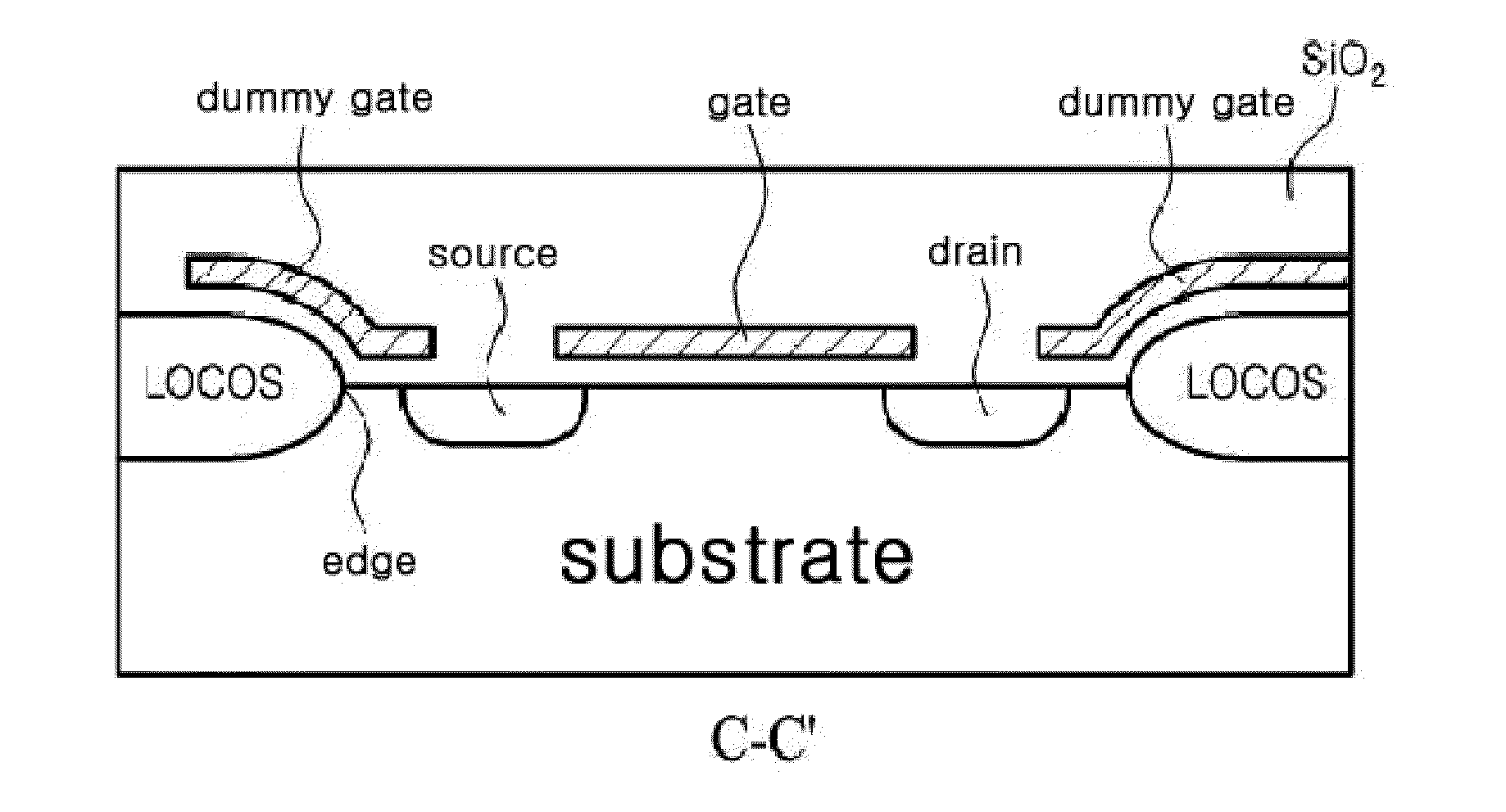
Radiation tolerant dummy gate-assisted n-MOSFET, and method and apparatus for modeling channel of semiconductor device
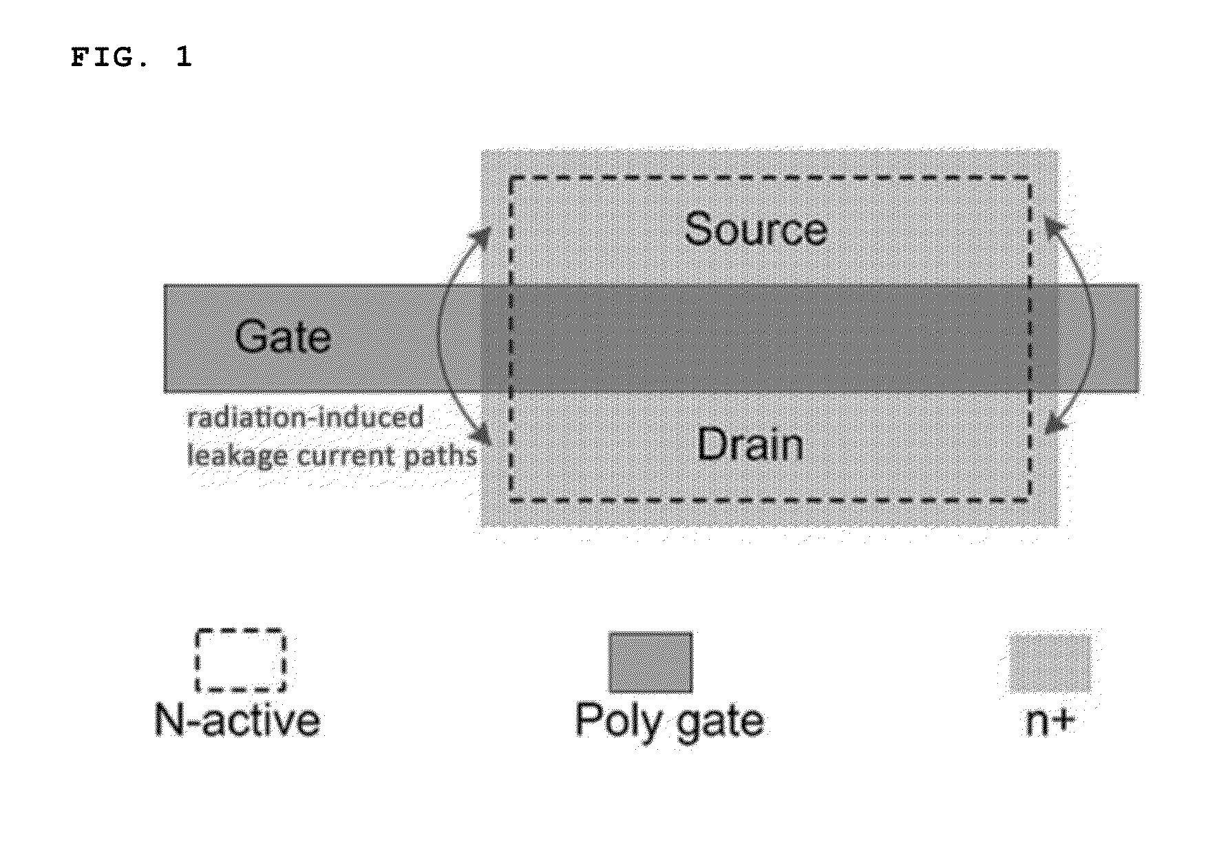
a technology of mosfet and gate-assisted n-mosfet, which is applied in the direction of transistors, electrical devices, semiconductor devices, etc., can solve the problems of inability to solve the desired channel region geometry, leakage current induced, and blockage of the turn-off operation of the mos
- Summary
- Abstract
- Description
- Claims
- Application Information
AI Technical Summary
Benefits of technology
Problems solved by technology
Method used
Image

Examples
first embodiment
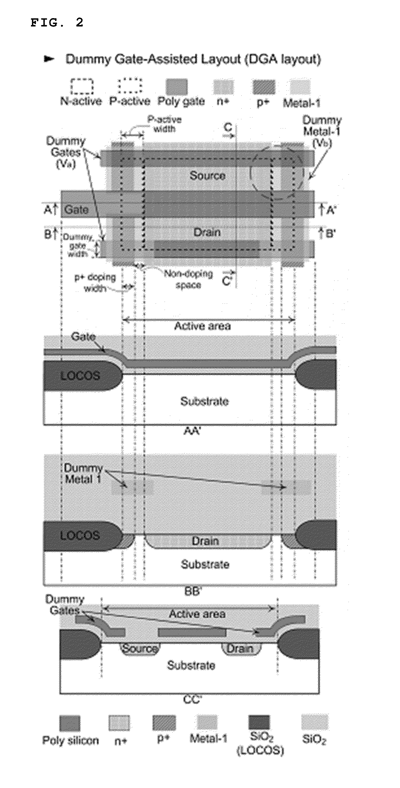
[0060]FIG. 5 shows a radiation tolerant DGA n-MOSFET layout according to the first embodiment of the present invention.
[0061]Referring to FIG. 5, in the first embodiment, the dummy poly gate layer 20, the dummy metal-1 layer 10, and the p-active layer and the p+ layer 30 are all used together as described before. In this case, each of these layers contributes to radiation tolerance, as described before. Particularly, at the p-active layer, the p+ layer 30 and the dummy metal-1 layer 10 may function to provide radiation resistance in an overlapping manner.
second embodiment
[0062]FIG. 6 shows a radiation tolerant DGA n-MOSFET layout according to the second embodiment of the present invention.
[0063]Referring to FIG. 6, in the second embodiment, only two layers of the dummy poly gate layer 20 and the dummy metal-1 layer 10 are used as described before. At the p-active layer, the dummy metal-1 layer 10 alone may function to impart radiation resistance. As the p+ layer and the dummy metal-1 layer 10 act on the same position, the dummy metal-1 layer 10 may be sufficient for radiation resistance as in the case of the second embodiment.
third embodiment
[0064]FIG. 7 shows a radiation tolerant DGA n-MOSFET layout according to the third embodiment of the present invention.
[0065]Referring to FIG. 7, in the third embodiment, only two layers of the dummy poly gate layer 20 and the p+ layer 30 are used as described before. At the p-active layer, the p+ layer 30 alone may function to impart radiation resistance. As the p+ layer 30 and the dummy metal-1 layer act on the same position, the p+ layer 30 may be sufficient for radiation resistance as in the case of the third embodiment.
PUM
 Abstract
Description
Claims
Application Information