Thin film transistor having oxide semiconductor layer

a thin film transistor and semiconductor layer technology, applied in semiconductor devices, instruments, electrical equipment, etc., can solve the problems of reducing the reliability of the transistor and deteriorating the electrical characteristics of the transistor, and achieve stable electrical characteristics, favorable electric characteristics, and high reliability

Active Publication Date: 2014-12-30
SEMICON ENERGY LAB CO LTD
View PDF132 Cites 50 Cited by
  • Summary
  • Abstract
  • Description
  • Claims
  • Application Information

AI Technical Summary

Benefits of technology

[0012]An object of one embodiment of the present invention is to provide an oxide semiconductor with a low density of localized states.
[0014]An object of one embodiment of the present invention is to provide a highly reliable semiconductor device which has stable electrical characteristics.
[0015]Therefore, an object of an embodiment of the present invention is to provide a semiconductor device which has favorable electric characteristics.
[0025]According to one embodiment of the present invention, an oxide semiconductor with a low density of localized states can be provided.
[0027]According to one embodiment of the present invention, a highly reliable semiconductor device which has stable electrical characteristics can be provided.
[0028]According to one embodiment of the present invention, a semiconductor device which has favorable electric characteristics can be provided.

Problems solved by technology

Accordingly, an increase in interface states leads to deterioration of the electrical characteristics of the transistor and a reduction in reliability of the transistor.

Method used


Image

  • Thin film transistor having oxide semiconductor layer
  • Thin film transistor having oxide semiconductor layer
  • Thin film transistor having oxide semiconductor layer

Examples


embodiment 1

[0067]In this embodiment, a transistor 100 is described as an example of a semiconductor device.

[1-1. Structural Example of Semiconductor Device]

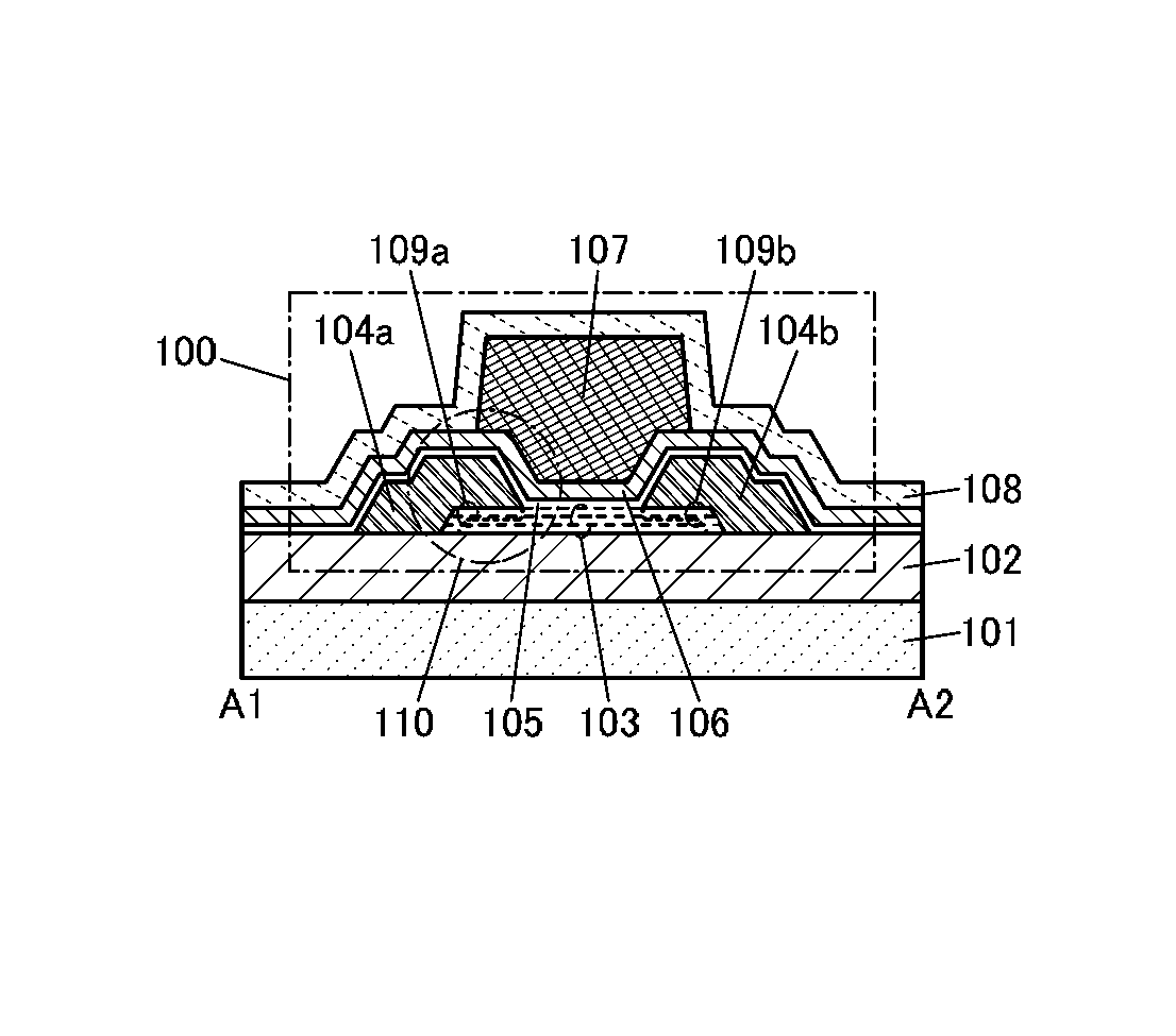
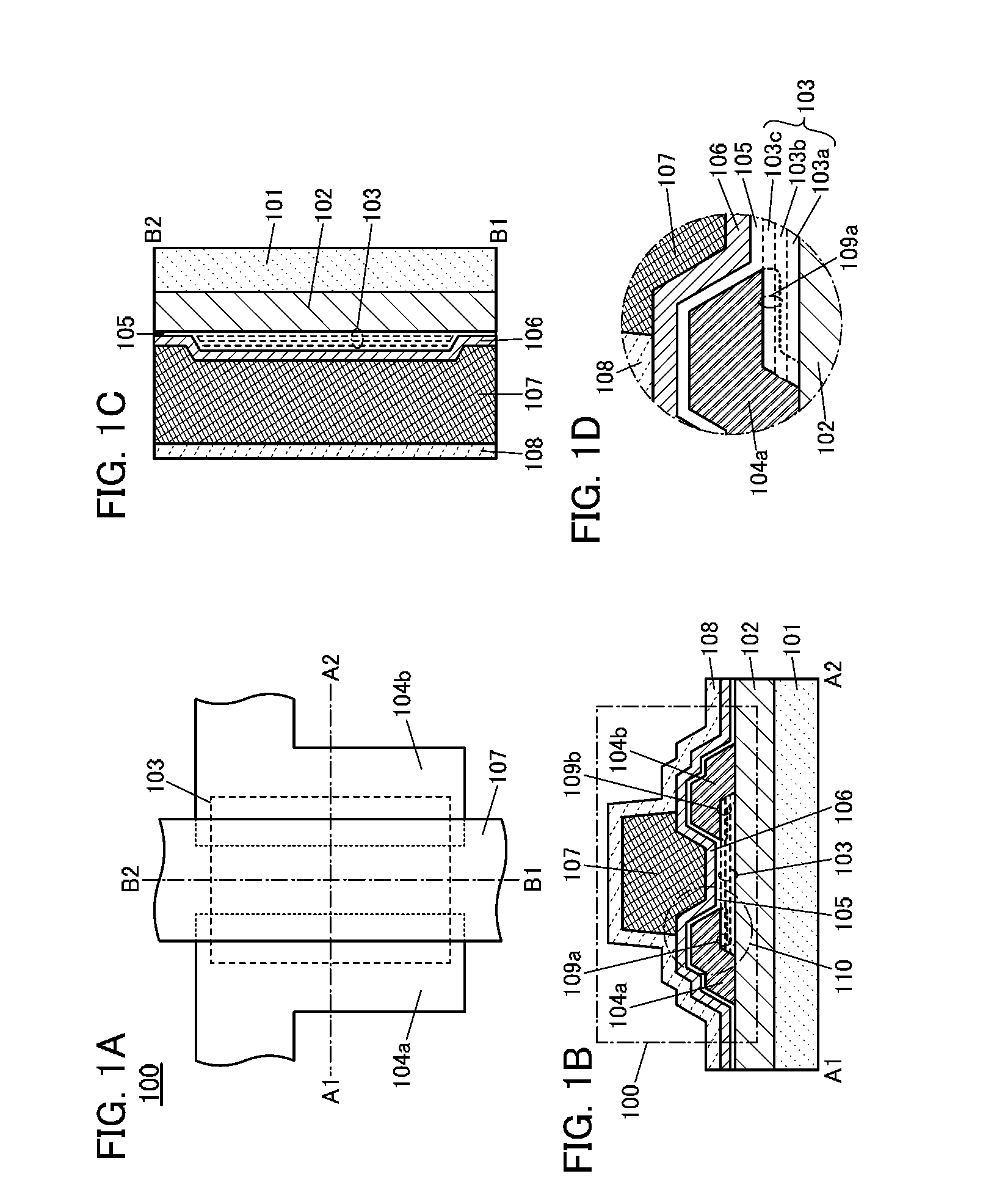
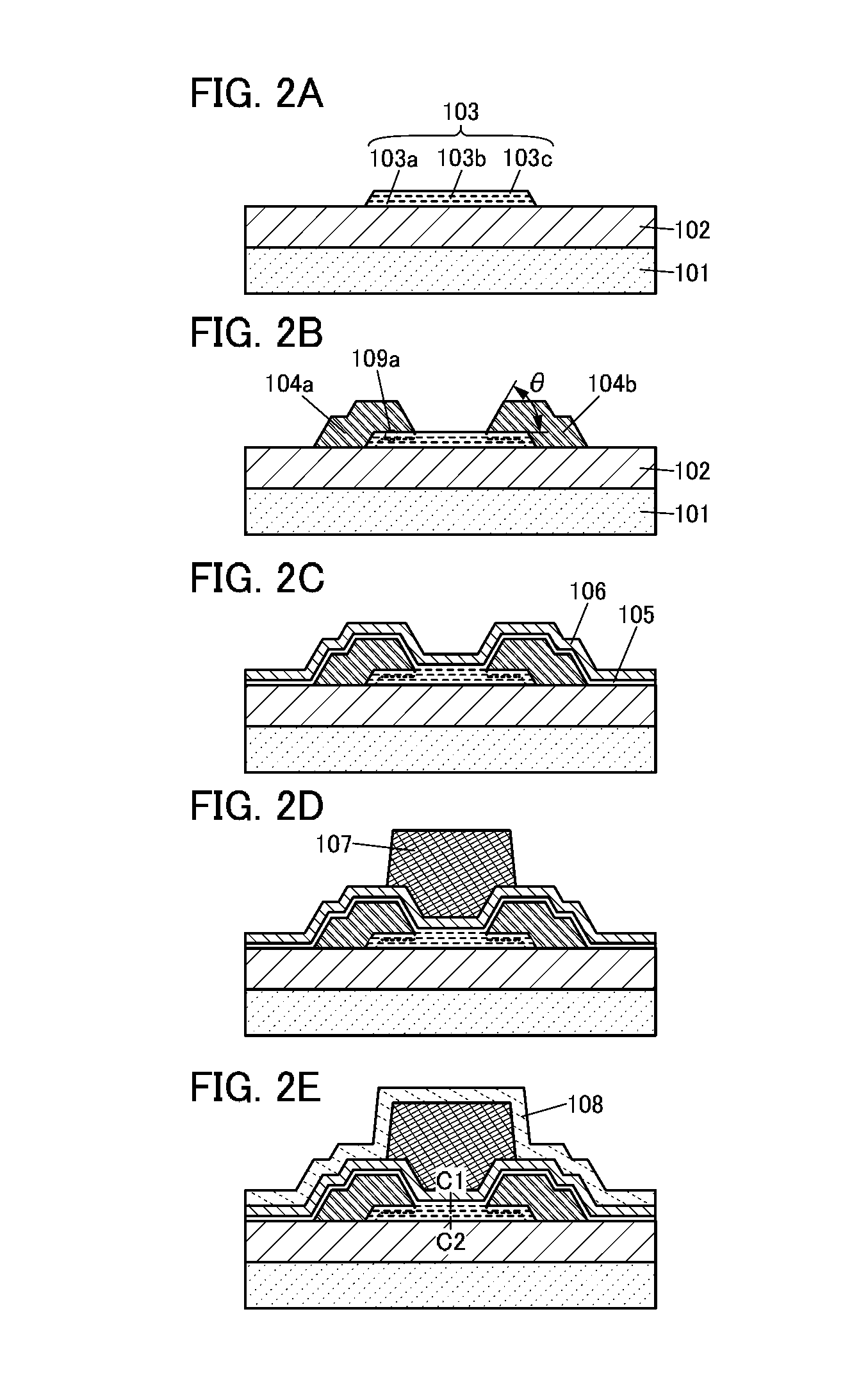
[0068]FIGS. 1A to 1D illustrate the transistor 100 of one embodiment of a semiconductor device. The transistor 100 is a top-gate transistor. FIG. 1A is a top view of the transistor 100. FIG. 1B is a cross-sectional view of a portion denoted by a dashed dotted line A1-A2 in FIG. 1A and FIG. 1C is a cross-sectional view of a portion denoted by a dashed dotted line B1-B2 in FIG. 1A. FIG. 1D is an enlarged view of a portion 110 in FIG. 1B. Note that some components are not illustrated in FIG. 1A.

[0069]The transistor 100 is formed over an insulating layer 102. The insulating layer 102 is formed over a substrate 101. The transistor 100 includes a stack 103 which is formed over the insulating layer 102 and includes a source electrode 104a and a drain electrode 104b which are formed over the stack 103. An oxide layer 105 is formed over the source e...

embodiment 2

[0274]In this embodiment, a transistor 150 which has a different structure from the transistor 100 described in the above embodiment is described.

[2-1. Structural Example of Semiconductor Device]

[0275]FIGS. 11A to 11C illustrate the transistor 150 of one embodiment of a semiconductor device. FIG. 11A is a top view of the transistor 150. FIG. 11B is a cross-sectional view of a portion denoted by a dashed dotted line A3-A4 in FIG. 11A and FIG. 11C is a cross-sectional view of a portion denoted by a dashed dotted line B3-B4 in FIG. 11A.

[0276]The transistor 150 is a top-gate transistor. The transistor 150 has substantially the same structure as the transistor 100 except the shapes of the insulating layer 106 and the oxide layer 105 in a cross-sectional structure.

[0277]The transistor 150 has a structure in which part of the insulating layer 106 and part of the oxide layer 105 which do not overlap with the gate electrode 107 are removed. Such a structure can prevent an increase in leakage...

embodiment 3

[0281]In this embodiment, a transistor 160 which has a different structure from the transistor described in the above embodiment is described.

[3-1. Structural Example of Semiconductor Device]

[0282]FIGS. 12A to 12C illustrate the transistor 160 of one embodiment of the present invention. FIG. 12A is a top view of the transistor 160. FIG. 12B is a cross-sectional view of a portion denoted by a dashed dotted line A5-A6 in FIG. 12A, and FIG. 12C is a cross-sectional view of a portion denoted by a dashed dotted line B5-B6 in FIG. 12A.

[0283]The transistor 160 is a top-gate transistor. The transistor 160 has substantially the same structure as the transistor 100 except the cross-sectional shapes of a source electrode and a drain electrode.

[0284]The edges of a source electrode 104as and a drain electrode 104bs in the transistor 160 each have a step-like shape. The step-like edges of the source electrode 104as and the drain electrode 104bs can lead to an improvement in coverage with a layer ...


PUM


Abstract

Oxide layers which contain at least one metal element that is the same as that contained in an oxide semiconductor layer including a channel are formed in contact with the top surface and the bottom surface of the oxide semiconductor layer, whereby an interface state is not likely to be generated at each of an upper interface and a lower interface of the oxide semiconductor layer. Further, it is preferable that an oxide layer, which is formed using a material and a method similar to those of the oxide layers be formed over the oxide layers Accordingly, the interface state hardly influences the movement of electrons.

Description

BACKGROUND OF THE INVENTION[0001]1. Field of the Invention[0002]The present invention relates to a semiconductor device and a method for manufacturing the semiconductor device.[0003]In this specification, a semiconductor device means all types of devices that can function by utilizing semiconductor characteristics, and a transistor, a semiconductor circuit, a memory device, an imaging device, a display device, an electro-optical device, an electronic appliance, and the like are all semiconductor device[0004]2. Description of the Related Art[0005]Attention has been focused on a technique for forming a transistor using a semiconductor thin film (also referred to as a thin film transistor (TFT)). The transistor is applied to a wide range of electronic devices such as an integrated circuit (IC) or an image display device. A silicon-based semiconductor material is widely known as a material for a semiconductor thin film applicable to a transistor. As another material, an oxide semiconduc...

Claims


Application Information

Patent Timeline
Patent Type & Authority Patents(United States)
IPC IPC(8): H01L29/24H01L29/12H01L29/66H01L29/786H01L29/10H01L29/49H01L27/12
CPCH01L29/4908H01L27/1225H01L29/247H01L29/7869H01L29/78693H01L29/66757H01L29/41733H01L29/66969H01L29/78618H01L29/78696G02F1/1368H01L29/42384H01L29/786H01L29/78645H01L29/78648
Inventor YAMAZAKI, SHUNPEI
Owner SEMICON ENERGY LAB CO LTD
Why Eureka
Try Eureka