Liquid crystal display device

a liquid crystal display and display device technology, applied in the field of liquid crystal display devices, can solve the problems of high driving voltage, and achieve the effect of reducing the amplitude voltage of an image signal written into a signal lin

Inactive Publication Date: 2015-01-06
SEMICON ENERGY LAB CO LTD
View PDF150 Cites 4 Cited by
  • Summary
  • Abstract
  • Description
  • Claims
  • Application Information

AI Technical Summary

Benefits of technology

[0016]In view of the above, it is an object of an embodiment of the present invention to provide a liquid crystal display device in which amplitude voltage of an image signal written into a signal line can be decreased.
[0038]According to another embodiment of the present invention, it is possible to provide a liquid crystal display device in which gate line inversion driving is performed and voltage of a scan line driver circuit and amplitude voltage of an image signal written into a signal line can be decreased, and a method for driving the liquid crystal display device.

Problems solved by technology

An in-plane switching (IPS) mode, which is described in Patent Document 1 and is a method for driving a blue-phase liquid crystal element, has a problem of high driving voltage in the case of AC driving.

Method used


Image

  • Liquid crystal display device
  • Liquid crystal display device
  • Liquid crystal display device

Examples


embodiment 1

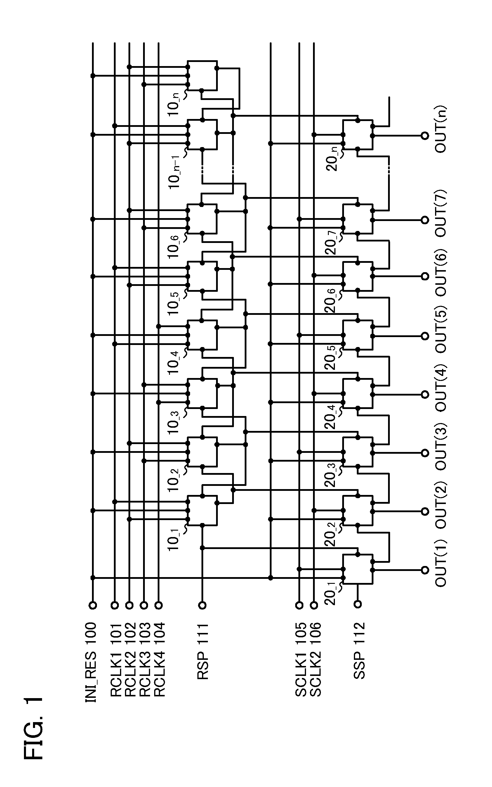
[0066]In this embodiment, as for a shift register which is provided in a common line driver circuit, examples of a reset pulse output circuit, a set pulse output circuit, and a shift register including the reset pulse output circuit and the set pulse output circuit will be described with reference to FIG. 1, FIGS. 2A and 2B, FIGS. 3A and 3B, FIG. 4, FIGS. 5A and 5B, FIGS. 6A and 6B, FIGS. 7A and 7B, FIGS. 8A and 8B, FIGS. 9A and 9B, FIGS. 10A and 10B, and FIG. 22.

[0067]First, the structure of a liquid crystal display device including a common line driver circuit provided with a shift register, which is described in this embodiment, will be described with reference to FIG. 22.

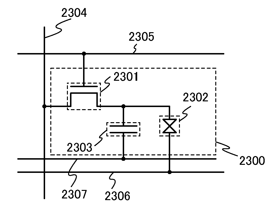
[0068]As illustrated in FIG. 22, the liquid crystal display device includes, over a substrate 2207, a pixel portion 2202 in which a plurality of pixels 2201 are arranged (arrayed) in matrix in a row direction and a column direction, and a signal line driver circuit 2203, a scan line driver circuit 2204, and a co...

embodiment 2

[0158]In this embodiment, the configuration of a shift register provided in a common line driver circuit, which is different from that in Embodiment 1, will be described.

[0159]The configuration of the shift register in this embodiment will be described with reference to FIG. 11. The shift register includes a first reset pulse output circuit 30—1 to an n-th reset pulse output circuit 30, (n is a natural number of greater than or equal to 2), and a first set pulse output circuit 20—1 to an n-th set pulse output circuit 20n.

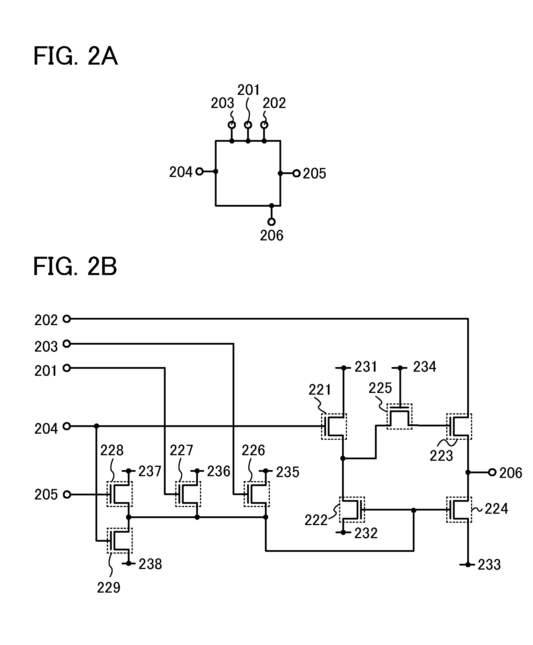
[0160]The reset pulse output circuit will be described with reference to FIGS. 12A and 12B.

[0161]In Embodiment 1, as shown in FIG. 1, each of the fifth input terminals 205 of the first reset pulse output circuit 10—1 to an (n−1)-th reset pulse output circuit 10—1 (n is a natural number of greater than or equal to 2) is connected to the first output terminal 206 of the reset pulse output circuit in the subsequent stage. In this embodiment, as shown in FIG. 11, each o...

embodiment 3

[0185]In this embodiment, the configuration of a shift register provided in a common line driver circuit, which is different from those in Embodiments 1 and 2, will be described with reference to FIG. 13, FIG. 14, and FIG. 15. In this embodiment, an example in which a first shift register and a second shift register are provided in the common line driver circuit will be described.

[0186]First, the configuration of the first shift register including a first reset pulse output circuit and a first set pulse output circuit will be described below.

[0187]The configuration of the first shift register in this embodiment will be described with reference to FIG. 13. The first shift register includes a first reset pulse output circuit 40—1 to an (2m−1)-th reset pulse output circuit 40—2m−1 (m is a natural number of greater than or equal to 2), and a first set pulse output circuit 50—1 to an (2m−1)-th set pulse output circuit 50—2m−1 (m is a natural number of greater than or equal to 2).

[0188]In...


PUM


Abstract

In a liquid crystal display device, amplitude voltage of an image signal written into a signal line can be decreased. A liquid crystal display device in which frame inversion driving is performed includes pixels each including a liquid crystal element and a transistor that controls voltage applied to a first electrode of the liquid crystal element. A scan line is electrically connected to gates of transistors in pixels in a corresponding row. A common line is electrically connected to second electrodes of liquid crystal elements in pixels in the corresponding row. In a first frame period, a first potential is sequentially supplied to the common lines in synchronization with sequential selection of the scan lines. In a second frame period adjacent to the first frame period, a second potential different from the first potential is sequentially supplied to the common lines in synchronization with sequential selection of the scan lines.

Description

BACKGROUND OF THE INVENTION[0001]1. Field of the Invention[0002]An embodiment of the present invention relates to a liquid crystal display device and an electronic device including the liquid crystal display device. In addition, an embodiment of the present invention relates to a method for driving a liquid crystal display device.[0003]2. Description of the Related Art[0004]Liquid crystal display devices ranging from a large display device such as a television receiver to a small display device such as a mobile phone have been spreading. From now on, products with higher added values will be needed and are being developed. In recent years, for high image quality and higher added values, a liquid crystal material exhibiting a blue phase (hereinafter also referred to as blue-phase liquid crystal) has attracted attention. Blue-phase liquid crystal can respond to an electric field at very high speed in comparison with conventional liquid crystal materials, and the use of blue-phase liqu...

Claims


Application Information

Patent Timeline
Patent Type & Authority Patents(United States)
IPC IPC(8): G06F3/038G09G3/36
CPCG09G3/3655G09G3/3614G09G2300/0434G09G2310/0286G11C19/28
Inventor MIYAKE, HIROYUKIKUSUNOKI, KOJI
Owner SEMICON ENERGY LAB CO LTD
Why Eureka
Try Eureka