

Receiver with enhanced clock and data recovery
a technology of enhanced clock and data recovery, applied in the direction of dc level restoring means or bias distorting correction, baseband system details, instruments, etc., can solve the problem of limited performance of conventional digital systems
- Summary
- Abstract
- Description
- Claims
- Application Information
AI Technical Summary
Benefits of technology
Problems solved by technology
Method used
Image

Examples
Embodiment Construction
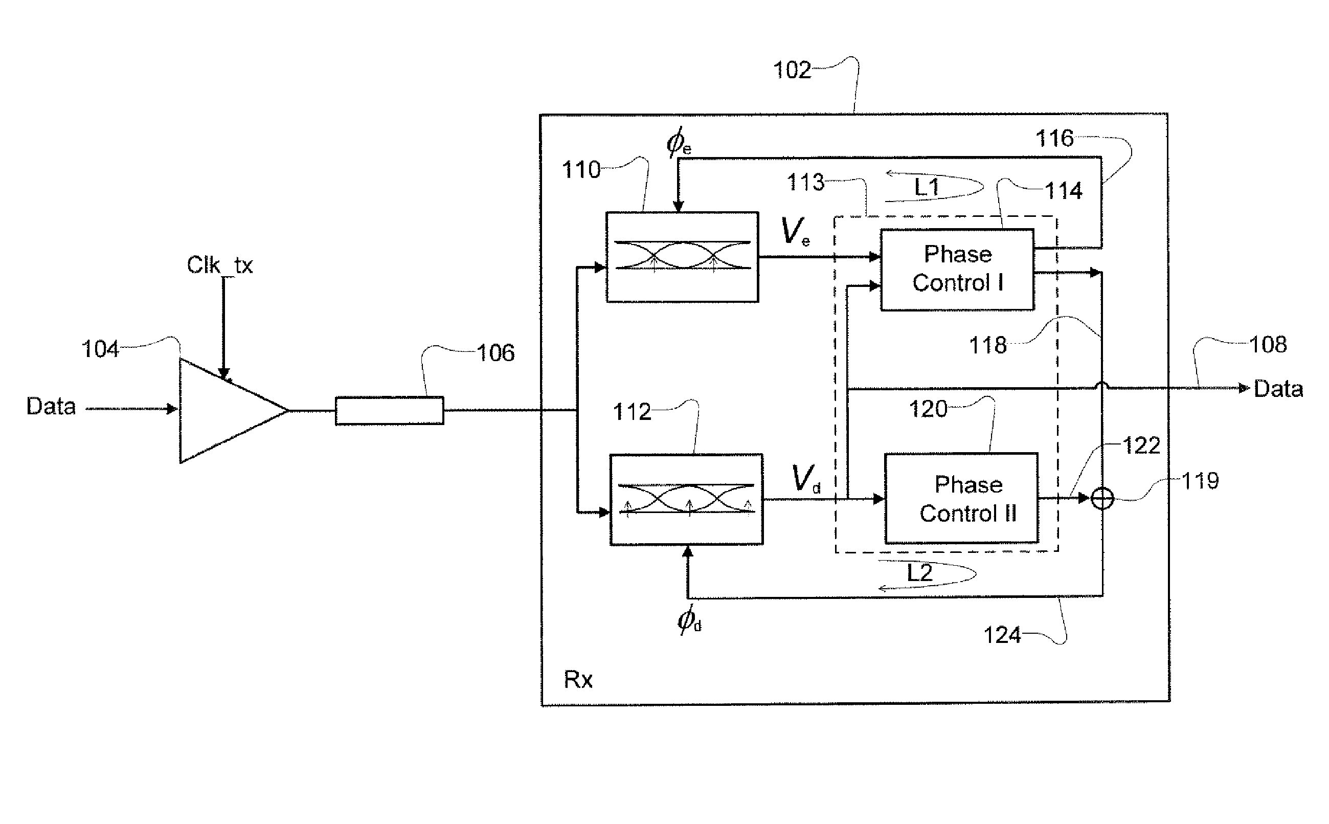
[0009]A receiver 102, such as the enhanced clock and data recovery receiver according to one embodiment of the present technology is illustrated in a data system of FIG. 1. The data system will typically include at least one transmitter 104. Transmitter 104 transmits data onto the signal path of a channel 106. Transmission of data is regulated by a transmit clock signal (shown as “Clk_tx” in FIG. 1) that is coupled with the transmitter 104. Signal path of the channel 106 may be a single ended signal path or differential signal paths, for example. Thus, the transmitter may be a differential signal transmitter or a single ended signal transmitter. Data signal 108 is a digital signal produced from the signal of the channel 106 and represents the recovered data that was transmitted from the transmitter 104.
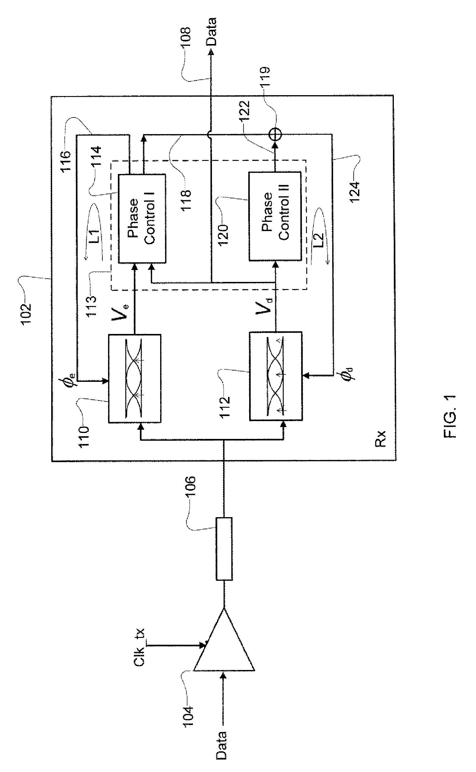
[0010]In the embodiment of FIG. 1, the receiver 102 typically includes edge sampler 110, data sampler 112, and one or more clock and data recovery elements 113. In the present embodim...
PUM
 Abstract
Description
Claims
Application Information