Wireless IC device

a wireless ic and wire-based technology, applied in the direction of semiconductor/solid-state device details, printed circuit non-printed electric components association, instruments, etc., can solve the problems of increasing the size of the printed wiring board itself and the inability to obtain radiation gain toward the surface layer in some cases, so as to prevent a reduction in radiation gain, improve the gain of high-frequency signal radiated from the first and second radiators, and efficient supply

Inactive Publication Date: 2015-02-03
MURATA MFG CO LTD
View PDF648 Cites 3 Cited by
  • Summary
  • Abstract
  • Description
  • Claims
  • Application Information

AI Technical Summary

Benefits of technology

[0008]In view of the above, preferred embodiments of the present invention provide a wireless IC device that improves radiation gain without increasing substrate size and also enables easily adjustment of impedance.
[0010]In the wireless IC device according to a preferred embodiment of the present invention, the wireless IC element is coupled to the first radiator via the feeding circuit including the first interlayer conductors, and is coupled to the second radiator via the first radiator and the second interlayer conductors. Therefore, high-frequency energy is efficiently supplied from the wireless IC element to the first and second radiators, and the gain of a high-frequency signal radiated from the first and second radiators is increased. Further, the first radiator is provided on the side of the second main surface of the substrate, and the second radiator is provided on the side of the first main surface of the substrate. Even if a surface layer of the wireless IC device includes components mounted thereon, therefore, it is possible to significantly reduce and prevent a reduction in radiation gain toward the surface layer, and the radiation gain is consequently improved. Particularly, the wireless IC element is preferably provided on the side of the first main surface of the substrate, and is coupled to the first radiator disposed on the second main surface. It is therefore possible to provide a relatively large area for arranging the feeding circuit, which is preferably located between the wireless IC element and the first radiator, without an increase in substrate area, and to achieve high impedance. Accordingly, it is easy to adjust the impedance of the feeding circuit.
[0011]Further, since the area in which the feeding circuit is provided is relatively large, it is possible, in a case in which the feeding circuit has a loop shape, to increase a magnetic flux passing through a loop, and the radiation gain is improved. Further, if the first interlayer conductors, the first radiator, the second interlayer conductors, and the second radiator are loop-shaped, a magnetic flux also passes through a loop defined by these conductors, and the radiation gain is further improved.
[0012]According to a preferred embodiment of the present invention, a wireless IC device that improves the radiation gain without increasing substrate size and that easily adjusts the impedance is obtainable, and is favorably usable in an RFID system.

Problems solved by technology

The increase in size of the antenna pattern, however, causes an increase in size of the printed wiring board itself.
Due to the influence of these mounted components, therefore, particularly a radiation gain toward the surface layer fails to be sufficiently obtained in some cases.

Method used


Image

  • Wireless IC device
  • Wireless IC device
  • Wireless IC device

Examples


first preferred embodiment

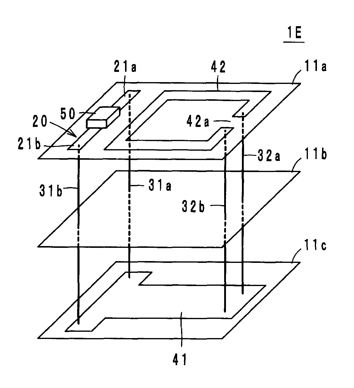
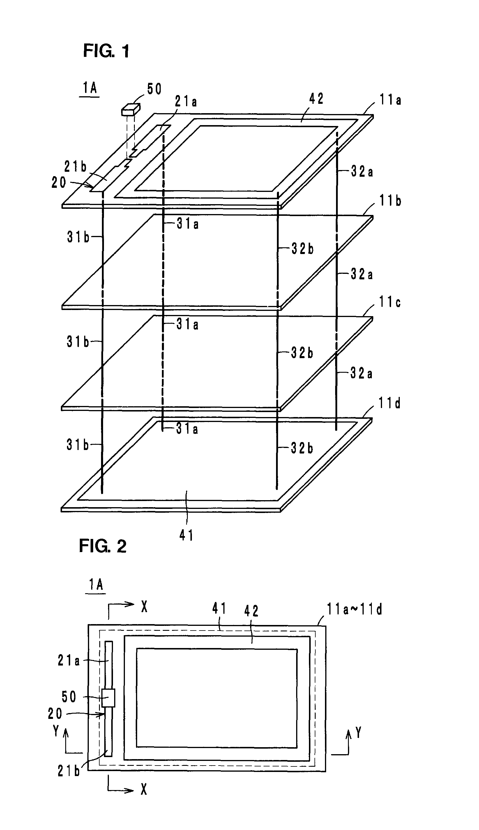
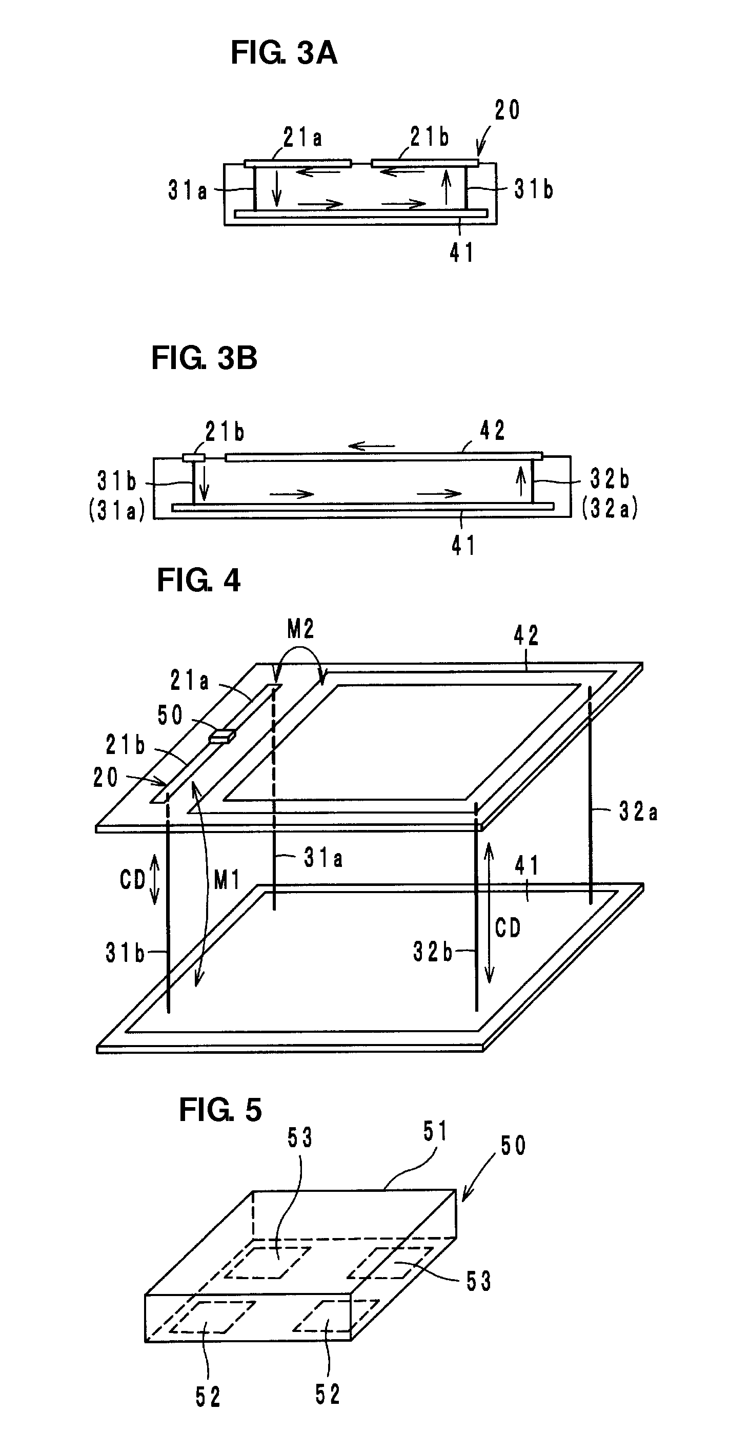
[0033]As illustrated in FIGS. 1 and 2, a wireless IC device 1A according to a first preferred embodiment of the present invention includes a multilayer substrate including base layers 11a, 11b, 11c, and 11d laminated on each other. The upper surface and the lower surface of the multilayer substrate will be referred to as the first main surface and the second main surface, respectively. On the side of the first main surface of the multilayer substrate, a wireless IC element 50 is provided and is arranged to process a high-frequency signal. On the side of the second main surface, a first radiator 41 is provided which is coupled to the wireless IC element 50 via a feeding circuit 20 including first interlayer conductors 31a and 31b. Further, on the side of the first main surface, a second radiator 42 is provided and is coupled to the first radiator 41 via second interlayer conductors 32a and 32b.

[0034]The wireless IC element 50, which processes a high-frequency signal, will be describ...

second preferred embodiment

[0058]As illustrated in FIG. 9, in a wireless IC device IB according to a second preferred embodiment of the present invention, the first radiator 41 is provided on the base layer 11d, and the second radiator 42 is provided on the base layer 11b. Further, a third radiator 43 is provided on the base layer 11c. Each of the radiators 41, 42, and 43 preferably is loop-shaped in a plan view. The configuration of the feeding circuit 20 is preferably the same as that of the first preferred embodiment, for example. The radiators 41, 42, and 43 are direct-current-coupled by the second interlayer conductors 32a and 32b in respective other side portions thereof.

[0059]The operational or functional effect of the wireless IC device 1B according to the second preferred embodiment of the present invention is basically similar to that of the first preferred embodiment of the present invention. With each of the radiators 41, 42, and 43 arranged into a loop shape in a plan view, a magnetic field is al...

third preferred embodiment

[0060]As illustrated in FIG. 10, in a wireless IC device 1C according to a third preferred embodiment of the present invention, the second radiator 42 is solidly provided in a large area on the base layer 11b, and this second radiator 42 and the first radiator 41 are direct-current-coupled by a multitude of second interlayer conductors 32a, 32b, and 32c. The third preferred embodiment of the present invention is similar to the first preferred embodiment of the present invention in the other configurations, and is also basically similar to the first preferred embodiment of the present invention in the operational or functional effect.

[0061]Particularly, if the second radiator 42 is solidly provided and connected to the first radiator 41 by the plurality of second interlayer conductors 32a, 32b, and 32c, as in the present third preferred embodiment of the present invention, the grounding function is reinforced. Further, in a side view, the first and second radiators 41 and 42 are conf...


PUM


Abstract

A wireless IC device that improves radiation gain without increasing substrate size and easily adjusts impedance, includes a multilayer substrate including laminated base layers. On a side of an upper or first main surface of the multilayer substrate, a wireless IC element is arranged to process a high-frequency signal. On a side of a lower or second main surface of the multilayer substrate, a first radiator is provided and is coupled to the wireless IC element via a feeding circuit including first interlayer conductors. On the side of the first main surface, a second radiator is provided and is coupled to the first radiator via second interlayer conductors.

Description

BACKGROUND OF THE INVENTION[0001]1. Field of the Invention[0002]The present invention relates to a wireless IC device, particularly to a wireless IC device preferably for use in an RFID (Radio Frequency Identification) system.[0003]2. Description of the Related Art[0004]In recent years, as an article information management system, an RFID system that has been in practical use performs non-contact communication using an electromagnetic field and transmits predetermined information between a reader-writer which generates an induced magnetic field and an RFID tag attached to an article. This RFID tag includes a wireless IC chip which stores predetermined information and processes a predetermined high-frequency signal and an antenna (radiator) which transmits and receives a high-frequency signal.[0005]The RFID system is in some cases used in information management of a printed wiring board included in various electronic devices. As this type of printed wiring board, those described in J...

Claims


Application Information

Patent Timeline
Patent Type & Authority Patents(United States)
IPC IPC(8): G06K19/06G06K19/07H01L23/66H01Q1/22H01Q1/38H01Q7/00H01Q21/30H05K1/18
CPCG06K19/0723H01Q1/2208H01Q1/38H01Q7/00H05K1/182H01Q21/30H01L23/66H01L2223/6677H01L2924/0002H01L2924/15311H01L2924/19105H01L2924/00
Inventor DOKAI, YUYAOZAWA, MASAHIRO
Owner MURATA MFG CO LTD
Why Eureka
Try Eureka