

Parasitic-patch-loaded high-gain microstrip antenna based on GaN processing technology
A parasitic patch and processing technology, applied in antennas, antenna grounding devices, electrical components, etc., can solve problems such as unfavorable antenna radiation, increase antenna size, and large silicon loss, and achieve simple structure and improved antenna radiation gain. , the effect of low cost
- Summary
- Abstract
- Description
- Claims
- Application Information
AI Technical Summary
Problems solved by technology
Method used
Image

Examples
Embodiment 1
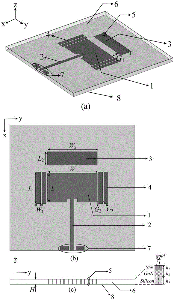
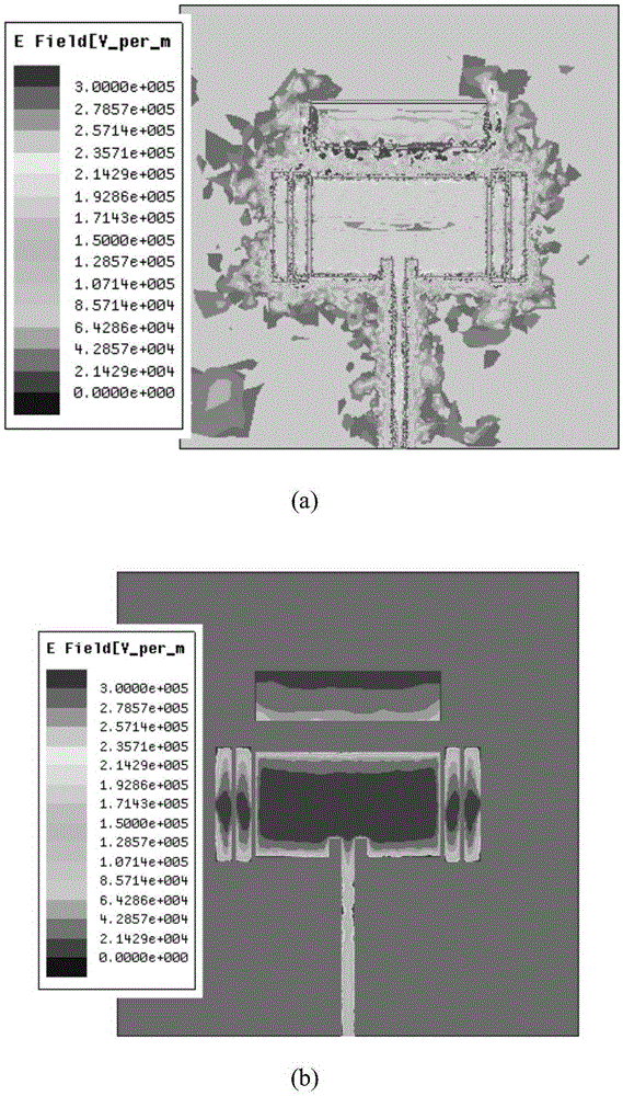
[0031] to combine figure 1 , the microstrip antenna includes a rectangular patch antenna 1, a feeding microstrip line 2, a parasitic patch 3 grounded at one end, a parasitic metal strip 4, a grounded metal post 5, a dielectric substrate 6, and a GSG structure required for probe measurement 7 and metal floor 8. The parasitic patch 3 with one end grounded is connected to the metal floor 8 through 13 grounded metal posts 5 . Two parasitic metal strips 4 are respectively printed along the non-radiating sides of the rectangular patch antenna 1 . Wherein the length L of the rectangular microstrip antenna 1 is 0.68mm (0.47λ g ), the width W is 1.2mm (0.83λ g ). The length L of a parasitic patch 3 grounded at one end 2 0.38mm (0.26λ g ), width W 2 1.2mm (0.83λ g ). The length L of the parasitic metal strip 4 1 0.75mm (0.52λ g ), width W 1 0.1mm (0.07λ g ). The gap width G between the rectangular patch antenna 1 and the parasitic patch 3 grounded at one end 1 0.2mm (0.14...
Embodiment 2
[0037] to combine Figure 5 , the microstrip antenna includes a rectangular patch antenna 1, a feeding microstrip line 2, a parasitic patch 3 grounded at one end, a parasitic metal strip 4, a grounded metal post 5, a dielectric substrate 6, and a GSG structure required for probe measurement 7 and metal floor 8. The parasitic patch 3 with one end grounded is connected to the metal floor 8 through 13 grounded metal posts 5 . Two parasitic metal strips 4 are respectively printed along the non-radiating sides of the rectangular patch antenna 1 . Wherein the length L of the rectangular microstrip antenna 1 is 0.67mm (0.46λ g ), the width W is 1.23mm (0.85λ g ). The length L of a parasitic patch 3 grounded at one end 2 0.3mm (0.2λ g ), width W 2 1.23mm (0.85λ g ). The length L of the parasitic metal strip 4 1 0.65mm (0.45λ g ), width W 1 0.07mm (0.05λ g ). The gap width G between the rectangular patch antenna 1 and the parasitic patch 3 grounded at one end 1 0.1mm (0....
Embodiment 3
[0042] to combine Figure 8 , the microstrip antenna includes a rectangular patch antenna 1, a feeding microstrip line 2, a parasitic patch 3 grounded at one end, a parasitic metal strip 4, a grounded metal post 5, a dielectric substrate 6, and a GSG structure required for probe measurement 7 and metal floor 8. The parasitic patch 3 with one end grounded is connected to the metal floor 8 through the ground metal post 5 . Two parasitic metal strips 4 are respectively printed along the non-radiating sides of the rectangular patch antenna 1 . Wherein the length L of the rectangular microstrip antenna 1 is 0.62mm (0.43λ g ), the width W is 0.8mm (0.55λ g ). The length L of a parasitic patch 3 grounded at one end 2 0.27mm (0.19λ g ), width W 2 0.8mm (0.55λ g ). The length L of the parasitic metal strip 4 1 0.75mm (0.52λ g ), width W 1 0.12mm (0.08λ g ). The gap width G between the rectangular patch antenna 1 and the parasitic patch 3 grounded at one end 1 0.15mm (0.1...
PUM
| Property | Measurement | Unit |
|---|---|---|
| Wide w | aaaaa | aaaaa |
| Gap width | aaaaa | aaaaa |
| Thickness | aaaaa | aaaaa |
Abstract
Description
Claims
Application Information