Standard cell for integrated circuit

a technology of integrated circuits and standard cells, which is applied in the direction of semiconductor devices, semiconductor/solid-state device details, electrical apparatus, etc., can solve the problems of increasing contact volume, and reducing the performance of transistors

Active Publication Date: 2015-02-24
STMICROELECTRONICS SRL
View PDF16 Cites 1 Cited by
  • Summary
  • Abstract
  • Description
  • Claims
  • Application Information

AI Technical Summary

Benefits of technology

[0005]According to one embodiment, a standard cell topology may be produced in sub-28-nanometer CMOS technology. For example, a standard cell topology may be produced in 20-nanometer CMOS technology, which may allow the performance of the transistors of this cell not to be degraded.
[0006]According to one embodiment, some of the gate contacts may be moved towards one of the ends of the cell, and some other of the gate contacts may be placed between the active zones to thereby allow the size of the active zones not to be reduced. This may, consequently, allow the performance of the transistors not to be degraded.
[0009]Moving the first line contacts towards the corresponding end of the cell, and placing the other line contacts between the two regions containing the active zones may allow this free space to be occupied to meet a minimum distance requirement between these two regions. This may also allow the area of the second region including, for example, the active zones of the nMOS transistors, not to be reduced.
[0012]Although it may be possible to place the second set of supply rails at the end of the cell, it may be particularly advantageous for this set to extend above the second region, thereby also providing a greater degree of freedom for the placement of these supply rails.
[0015]This placement asymmetry of the two regions of semiconductor zones is possible because of the distribution of the line contacts mentioned above, and it may especially allow active-zone areas compatible with the desired performance of the transistors to be preserved.
[0016]According to another aspect, an integrated circuit may include several standard cells, such as, for example, the standard cells defined above. In one embodiment, in particular when these cells are input / output cells, the first set of supply rails and the second set of supply rails of a cell may respectively make contact with the first set of supply rails and the second set of supply rails of an adjacent cell. This allows electrical continuity of the supply rails from one cell to another to be ensured.

Problems solved by technology

For sub-28-nanometer technology, the size of the contacts generally increases, and thus, it may then no longer be possible to place these contacts side by side on the parallel gate lines.
However, design constraints would then require the size of these active zone regions, and therefore consequently, the performance of the transistors, to be reduced.

Method used


Image

  • Standard cell for integrated circuit
  • Standard cell for integrated circuit
  • Standard cell for integrated circuit

Examples


Embodiment Construction

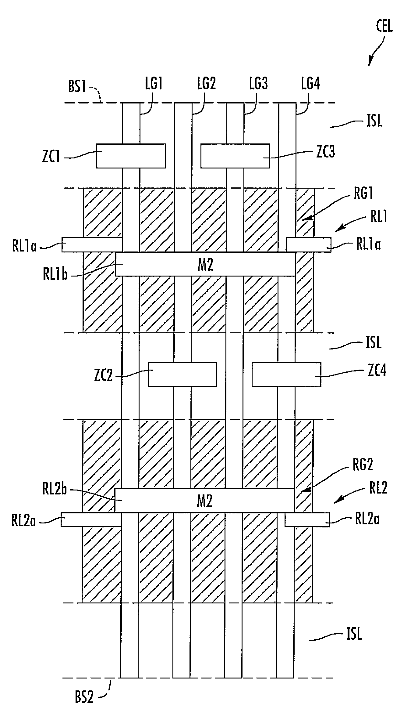
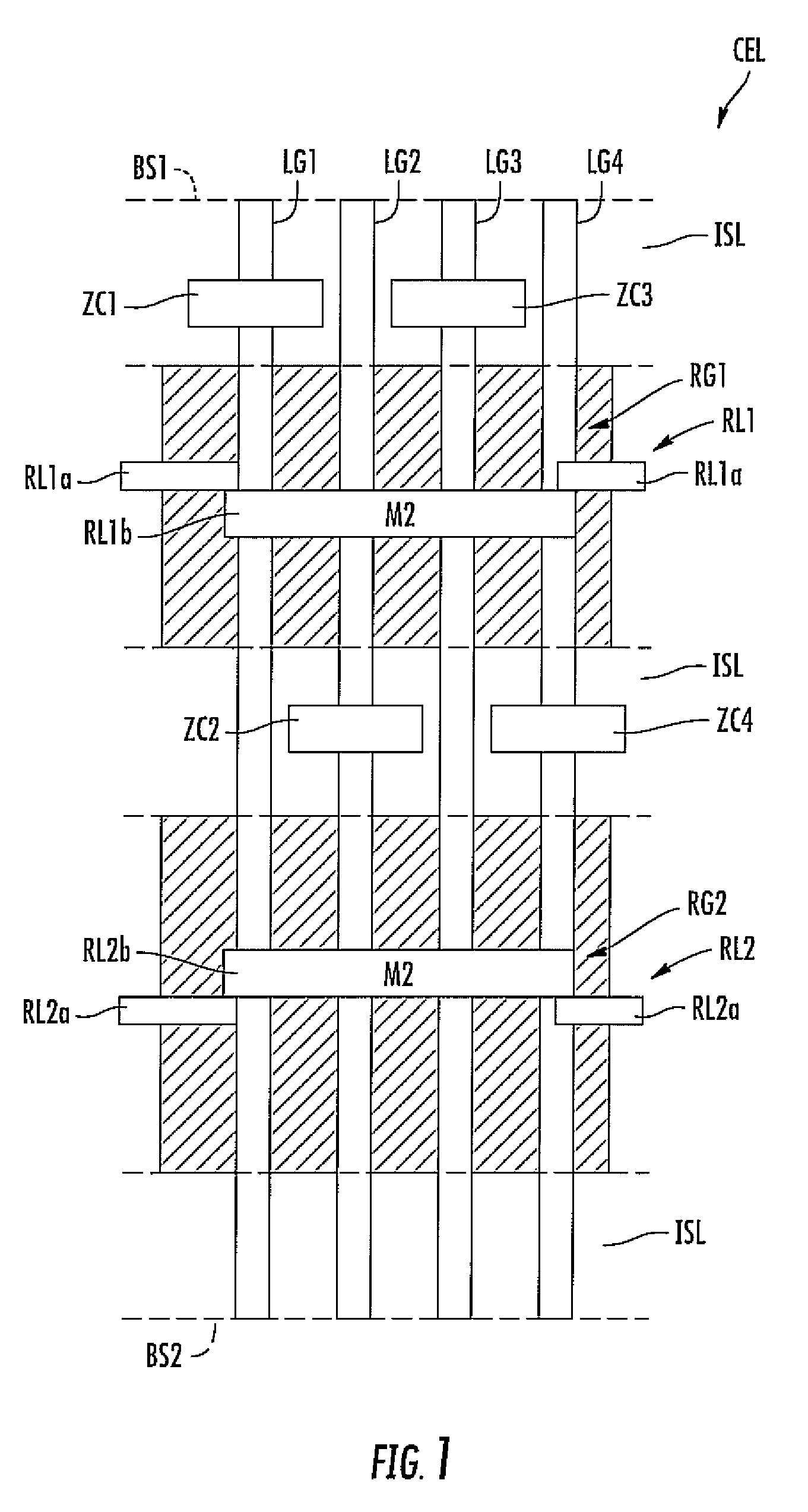
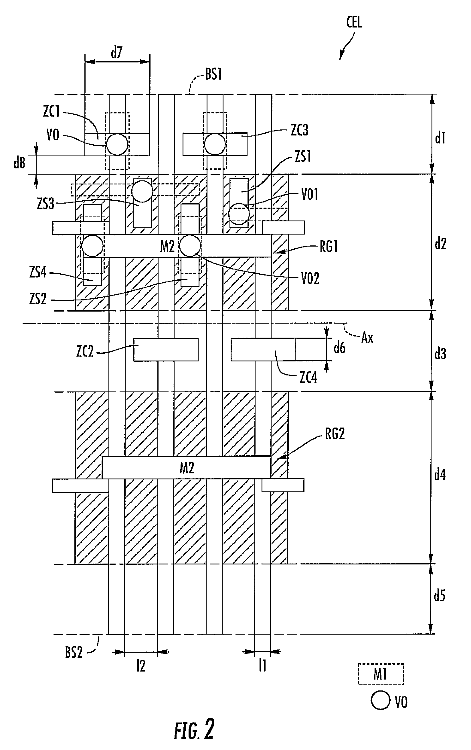
[0021]Although the invention applies to any standard cell produced in sub-28-nanometer technology, and especially sub-20-nanometer or 20-nanometer technology, FIGS. 1 and 2 schematically illustrate an exemplary topology for a standard cell produced in 20-nanometer CMOS technology.

[0022]The standard cell CEL is illustratively an input / output cell comprising pMOS transistors and nMOS transistors. In the illustrated example, the source and drain active zones of the pMOS transistors are located in the first region RG1, whereas the source and drain active zones of the nMOS transistors are located in the second region RG2. The regions RG1 are surrounded by isolating regions ISL, for example, shallow trench isolation (STI) regions.

[0023]The references LG1, LG2, LG3, and LG4 denote lines, for example, made of polycrystalline silicon, forming the transistors of the cell CEL gate lines. These gate lines are parallel. The cell CEL comprises, by way of non-limiting example, four gate lines. The...


PUM


Abstract

An integrated circuit (IC) cell may include first and second semiconductor regions, and parallel electrically conductive lines extending above the first and second semiconductor regions. The IC cell may further include electrically conductive line contacts electrically connected to the parallel electrically conductive lines, and may include at least one first line contact between the first semiconductor region and a corresponding end of the IC cell, and at least one second line contact between the first semiconductor region and the second semiconductor region. Adjacent ones of the electrically conductive lines may be respectively coupled to one of the at least one first line contact and to one of the at least one second line contact.

Description

FIELD OF THE INVENTION[0001]The invention relates to integrated circuits, and, more particularly to standard cells, for example input / output cells.BACKGROUND OF THE INVENTION[0002]Standard cells are generally produced using complementary metal oxide semiconductor (CMOS) technology, and may be pre-optimized cells saved in cell libraries. Thus, the designer of an integrated circuit may use standard cells by placing them and interconnecting them based upon the structure and functionality of the integrated circuit to be designed.[0003]Conventional topology standard cells may be used down to a 28-nanometer technology node size, which corresponds to the line width, and generally corresponds to the channel length or gate width of a transistor produced in this technology. More precisely, conventional topology input / output standard cells, for example, may comprise n-channel metal-oxide-semiconductor field-effect (nMOS) transistors and p-channel metal-oxide-semiconductor field-effect (pMOS) t...

Claims


Application Information

Patent Timeline
Patent Type & Authority Patents(United States)
IPC IPC(8): H01L23/52H01L23/528H01L27/02H01L27/118
CPCH01L27/11807H01L27/0207H01L23/5286H01L2924/0002H01L2924/00
Inventor SENGUPTA, RWIKGUPTA, ROHIT KUMARGOYAL, MITESHMENUT, OLIVIER
Owner STMICROELECTRONICS SRL
Why Eureka
Try Eureka