LED lens and light source device using the same

a technology of led light source and lens, which is applied in the direction of semiconductor devices for light sources, lighting and heating apparatus, instruments, etc., can solve the problems of difficult to achieve the requirement of high scattering ability, difficult to have both perfect scattering ability and perfect uniformity of scattering properties, etc., to improve the light emission angle of light source devices, reduce the number of led light source devices, and improve the color uniformity of light source devices

Inactive Publication Date: 2015-03-03
E PIN OPTICAL IND
View PDF11 Cites 21 Cited by
  • Summary
  • Abstract
  • Description
  • Claims
  • Application Information

AI Technical Summary

Benefits of technology

[0011]The main purpose of the present invention is to provide an LED lens and a light source device applied to an LED backlight module or other illumination devices. Whereby a light pattern that the luminous intensity of the paraxial zone thereof is lower than the luminous intensity of the off-axis zone thereof is formed; the light emission angle and uniformity of the light illumination are improved. Therefore, the present invention is able to improve the display quality, to reduce chromatic aberration and to meet the requirement of even light distribution, high scattering ability, becoming thinner, and effectively reduce the number of the LED light source device and thus reduce the volume of the LED backlight, the heat accumulation in the backlight module and costs.

Problems solved by technology

However, although the light pattern generated by the light source device 1 gives lower intensities in the paraxial region, the light source device 1 still can't solve the problem of having bright dots in the paraxial region on the illuminated object.
In a result, the light source device 1 is hard to have both the perfect scattering ability and the perfect uniformity of scattering property.
A light source device disclosed in U.S. Pat. No. 7,621,657 is similar to the light source device 1 disclosed in U.S. Pat. No. 7,348,723, it also has the shortcomings that the paraxial zone of the light source device is too bright and it is difficult to achieve the requirement of high scattering ability.
In addition, due to a concave surfaces of the lens make light away from the optical axis of the light source device be refract to further close to the optical axis; and a convex surfaces of the optical lens make the incident light be refract to further away from the optical axis, this type light source device has the shortcomings of uneven light distribution and deficient scattering ability.
However, such optical lens is still hard to achieve the requirement of making display monitors using the optical lens be thinner since the light pattern of these prior art is wider distribution cause lower intensities effect in the paraxial region.
In a result, such optical lens is not applicable to use in thinner display monitors.
However, U.S. Pat. Nos. 7,474,475 and 7,746,565 are unable to provide even light pattern in practice, and such lenses are hard to process, and become thicker and low precision as its complex spherical surface.
If LED light source devices applied to a LCD display have design deficiency, they may cause the problems of bright dot, chromatism, requirement of high density lay-out or requirement of disposing other elements for promoting even light distribution.
Wherein, when an LED light source device has a problem that the paraxial zone of the light source device is too bright, it may cause chromatism thereby affecting the color rendering of the LCD display.
Besides, requirement of high density lay-out leads to increment of manufacturing cost, accumulation of heat and affects the device lifetime; requirement of disposing other elements further leads to increment of volume or weight of the LCD display.

Method used


Image

  • LED lens and light source device using the same
  • LED lens and light source device using the same
  • LED lens and light source device using the same

Examples


first embodiment

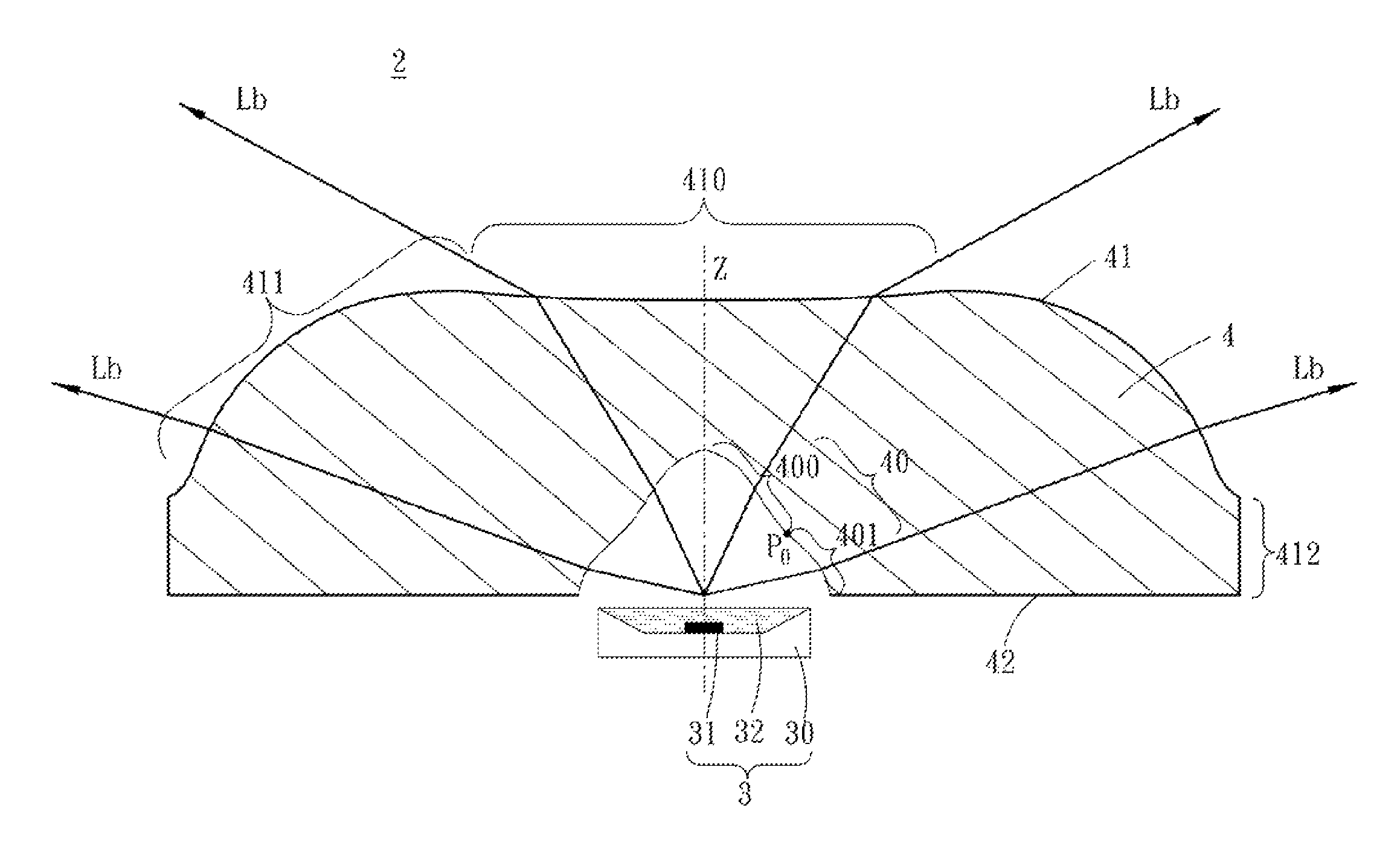
[0087]Please refer to FIGS. 8 and 9, they are a cross-sectional view illustrating a light source device of the present invention thereof and a polar candela distribution plot thereof, respectively.

[0088]In the Table (1) listed below, there are shown the coefficients of the aspheric surface formula (6) constituting the light emitting surface 41 of the LED lens 4 in the first embodiment:

[0089]

TABLE (1)cKA2A4A60.0110−8.188E−032.345E−02−3.123E−03A8A10A12A14A161.865E−04−6.214E−061.187E−07−1.215E−095.164E−12

[0090]In the Table (2) listed below, there are shown data referred to FIG. 5 and the refractive index (Nd) of the LED lens 4 in the first embodiment:

[0091]

TABLE (2)OI0OP0m′cosθ0(mm)(mm)tanθk(mm)cosθctanθe0.6681.8691.3411.0250.897−0.0596.224L3REhRII0E0L2(mm)(mm)(mm)(mm)(mm)(mm)Nd3.61515.0000.6963.5002.1990.5811.490

[0092]In the first embodiment, the LED lens 4 is made from PMMA having a refraction index of 1.49. The effective divergence angle of the light source device 2 using the LED l...

second embodiment

[0097]Please refer to FIGS. 10 and 11, they are a cross-sectional view illustrating a light source device of the present invention thereof and a polar candela distribution plot thereof, respectively.

[0098]In the Table (3) listed below, there are shown the coefficients of the aspheric surface formula (6) constituting the light emitting surface 41 of the LED lens 4 in the second embodiment:

[0099]

TABLE (3)cKA2A4A6−6.418E+12−4.504E+041.561E−022.308E−03−2.770E−04A8A10A12A148.028E−06−4.706E−08−1.562E−091.907E−11

[0100]In the Table (4) listed below, there are shown data referred to FIG. 5 and the refractive index (Nd) of the LED lens 4 in the second embodiment:

[0101]

TABLE (4)OI0OP0m′cosθ0(mm)(mm)tanθk(mm)cosθctanθe0.6681.8691.3411.0250.897−0.05919.559L3REhRII0E0L2(mm)(mm)(mm)(mm)(mm)(mm)Nd3.435150.6963.52.1990.1761.49

[0102]In the second embodiment, the LED lens 4 is made from PMMA having a refraction index of 1.49. The effective divergence angle of the light source device 2 using the LED l...

third embodiment

[0106]Please refer to FIGS. 12 and 13, they are a cross-sectional view illustrating a light source device of the present invention thereof and a polar candela distribution plot thereof, respectively.

[0107]In the Table (5) listed below, there are shown the coefficients of the aspheric surface formula (6) constituting the light emitting surface 41 of the LED lens 4 in the third embodiment:

[0108]

TABLE (5)cKA2A4A6−6.418E+12−2.975E+041.957E−022.253E−03−2.770E−04A8A10A12A148.017E−06−4.706E−08−1.562E−091.907E−11

[0109]In the Table (6) listed below, there are shown data referred to FIG. 5 and the refractive index (Nd) of the LED lens 4 in the third embodiment:

[0110]

TABLE (6)OI0OP0m′cosθ0(mm)(mm)tanθk(mm)cosθctanθe0.6052.3001.5980.9550.9930.22416.664L3REhRII0E0L2(mm)(mm)(mm)(mm)(mm)(mm)Nd3.52414.800.7673.81.90.2111.51

[0111]In the third embodiment, the LED lens 4 is made from transparent resin material having a refraction index of 1.51. The effective divergence angle of the light source devic...


PUM


Abstract

The present invention discloses an LED lens and a light source device using the same. The light source device includes the LED lens and a LED. The LED lens comprises a light incident surface, a light emitting surface, and a bottom surface. The light emitting surface includes a recession portion disposed at the central thereof and a convex portion connected to the recession portion. The light incident surface is a concave surface and comprises a first optically active area and a second optically active area. The first optically active area is disposed at the central of the light incident surface; the second optically active area is connected to the first optically active area and the bottom surface. At the junction between the first optically active area and the second optically active area, it is an optical path inversion point that is disposed satisfying specific condition.

Description

FIELD OF THE INVENTION[0001]The present invention relates to a lens and a light source device using the same, and more particularly to an LED lens and a light source device applied for various illumination devices using light-emitting diodes (LEDs) as light source.BACKGROUND OF THE INVENTION[0002]LCD displays are widely used in TVs, notebook computers, PCs, mobile phones, and other electronic products with display function. In an LCD display, cold cathode fluorescent lamps (CCFLs), field-effect light-emitting devices (EL), light-emitting diodes, or other elements capable of emitting a visible light are used as a backlight. In recent years, LED has gradually been a preferred backlight source instead of CCFLs because it has many advantage including: long lifetime (about 100,000 hours), capable of optimizing color gamut, small size / design flexibility, driven by low-voltage power supply, quicker turn-on time, without an inverter, operated efficiently over a wider temperature range and s...

Claims


Application Information

Patent Timeline
Patent Type & Authority Patents(United States)
IPC IPC(8): F21V3/00F21V5/00F21V5/04G02B3/02G02B13/18F21Y101/02G02B3/04G02B19/00G02B27/09H01L33/58
CPCG02B19/0014F21V5/046G02B3/04F21V5/04G02B27/0955H01L33/58G02B19/0061G02B19/0071F21Y2101/02F21Y2115/10
Inventor WANG, CHIH-PENGCHEN, HUANG-CHANGHSU, KUO-HSUANLEE, JUI-WEN
Owner E PIN OPTICAL IND
Why Eureka
Try Eureka