
Patterned substrate design for layer growth

a technology of patterned substrates and substrates, applied in the direction of basic electric elements, instruments, energy-based wastewater treatment, etc., can solve the problems of affecting the optical properties of materials, and affecting so as to improve the growth rate of semiconductor layers

Active Publication Date: 2015-03-17
SENSOR ELECTRONICS TECH
View PDF24 Cites 20 Cited by
  • Summary
  • Abstract
  • Description
  • Claims
  • Application Information

AI Technical Summary

Benefits of technology

The patterned substrate enhances light extraction and reduces stress in semiconductor layers, improving the efficiency and performance of emitting devices by allowing more light to escape and minimizing dislocations, thereby increasing the output power and reducing Fresnel losses.

Problems solved by technology

Changes in molar fractions of semiconductor alloys can allow for band gap control, but can lead to abrupt changes in the optical properties of the materials and result in light trapping.
A small TIR angle results in a large fraction of light rays reflecting from the interface boundaries, thereby leading to light trapping and subsequent absorption by layers or LED metal contacts.
Nevertheless, light only can be partially transmitted through the interface, even if it does not undergo TIR, due to Fresnel losses.

Method used


Image

  • Patterned substrate design for layer growth
  • Patterned substrate design for layer growth
  • Patterned substrate design for layer growth

Examples


second embodiment

[0041]FIGS. 5 and 6 show a side view and a two dimensional top view, respectively, of an illustrative patterned surface 40B of a substrate 12 (FIG. 1) according to a In this case, the patterned surface 40B includes a top surface 42 into which a plurality of openings 44 are formed. The openings 44 can be spaced from one another by a distance less than approximately twice a diameter of a top opening 45. In an embodiment, each opening 44 can have a top opening 45 of a diameter of approximately 2.0 μm and a bottom surface 47 having a diameter of approximately 1.5 μm. Furthermore, the openings 44 can be spaced from one another by approximately 3.5 μm center to center. As illustrated in FIG. 6, the openings can have substantially circular cross sections and be formed in a hexagonal pattern. However, it is understood that the openings 44 can comprise any combination of one or more of various types / shapes of cross-sectional patterns and form any type of pattern.

[0042]The patterned surfaces...

third embodiment

[0047]In an embodiment, a surface of a substrate 12 can include multiple patterns. For example, FIG. 10 shows a two dimensional top view of an illustrative patterned surface of a substrate 12 according to a In this case, the substrate 12 includes a plurality of stripes, such as stripes 70A and 70B, of an isolating material. In an embodiment, the isolating material comprises silicon dioxide. As illustrated, the stripes 70A, 70B can form a plurality of regions, such as regions 72A and 72B, each of which is isolated from another region by the stripes 70A, 70B. Each region 72A, 72B can comprise a patterned surface configured as described herein. Furthermore, the plurality of regions 72A, 72B can include patterned surfaces formed using a different solution and / or having different attributes. In this manner, each region 72A, 72B can comprise a configuration, which is suitable for stress reduction through lateral epitaxial overgrowth, selective area growth, selective polycrystalline growt...


PUM

PropertyMeasurementUnit
sizeaaaaaaaaaa
sizeaaaaaaaaaa
root mean square roughnessaaaaaaaaaa

Abstract

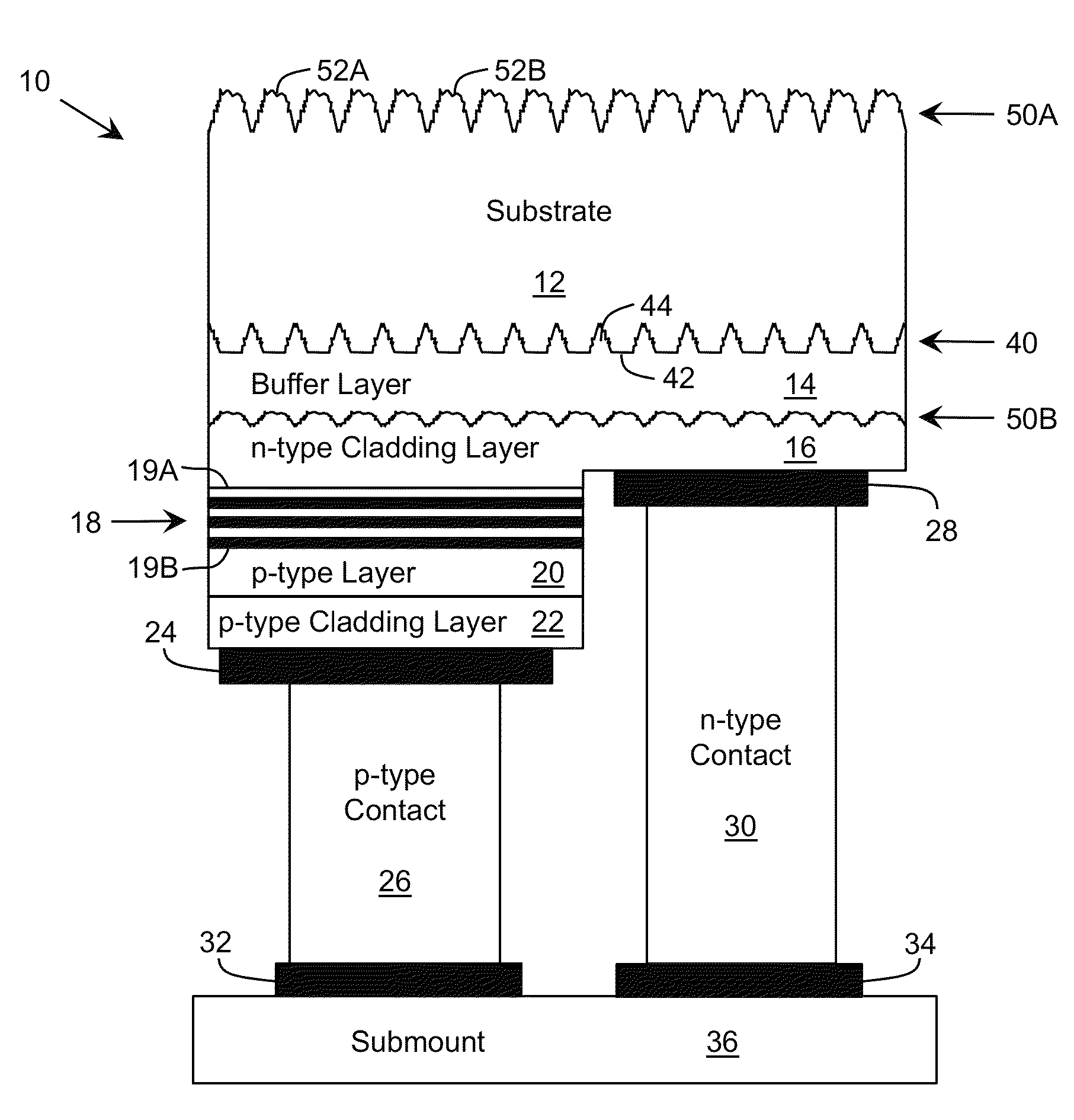
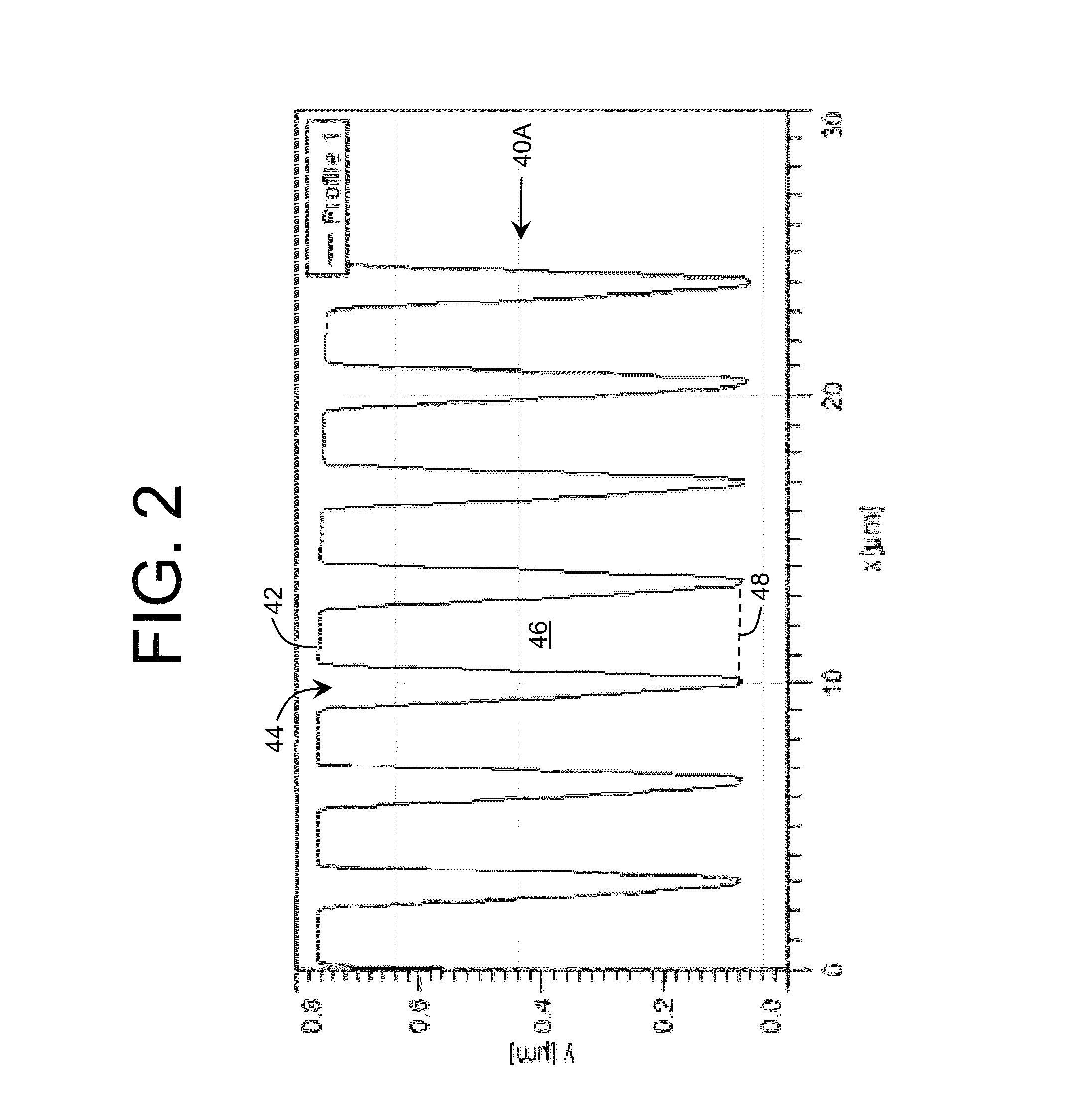
A patterned surface for improving the growth of semiconductor layers, such as group III nitride-based semiconductor layers, is provided. The patterned surface can include a set of substantially flat top surfaces and a plurality of openings. Each substantially flat top surface can have a root mean square roughness less than approximately 0.5 nanometers, and the openings can have a characteristic size between approximately 0.1 micron and five microns.

Description

REFERENCE TO RELATED APPLICATIONS[0001]The current application claims the benefit of U.S. Provisional Application No. 61 / 531,440, titled “Light Emitting Diodes with Optimal Patterned Substrate for Growing Nitride Based Semiconductor Layers,” which was filed on 6 Sep. 2011, and which is hereby incorporated by reference. Aspects of the invention also are related to U.S. patent application Ser. No. 13 / 524,350, titled “Device with Inverted Large Scale Light Extraction Structures,” which was filed on 15 Jun. 2012, and U.S. patent application Ser. No. 13 / 517,711, titled “Emitting Device with Improved Extraction,” which was filed on 14 Jun. 2012, both of which are hereby incorporated by reference.GOVERNMENT LICENSE RIGHTS[0002]This invention was made with Federal government support under Contract No. W911NF-10-2-0023 awarded by Defense Advanced Research Projects Agency (DARPA). The government has certain rights in the invention.TECHNICAL FIELD[0003]The disclosure relates generally to semic...

Claims


Application Information

Patent Timeline
Patent Type & Authority Patents(United States)
IPC IPC(8): H01L33/00H01L21/02H01L33/22
CPCH01L21/0237H01L21/0242H01L21/0243H01L33/22H01L21/0254H01L21/02639H01L21/0265H01L21/02458H01L2224/16225Y02W10/37
Inventor SHATALOV, MAXIM SJAIN, RAKESHYANG, JINWEISHUR, MICHAELGASKA, REMIGIJUS
Owner SENSOR ELECTRONICS TECH
Learn More