Organic light emitting diode display and method of fabricating the same

a light-emitting diode and organic technology, applied in the direction of thermoelectric device junction materials, electrical apparatus, semiconductor devices, etc., can solve the problems of unwanted capacitance between lines and dark spots, and achieve the effect of reducing unwanted capacitance, reducing unwanted capacitance, and maintaining film uniformity of the first medium layer

Active Publication Date: 2015-03-24
SAMSUNG DISPLAY CO LTD
View PDF16 Cites 12 Cited by
  • Summary
  • Abstract
  • Description
  • Claims
  • Application Information

AI Technical Summary

Benefits of technology

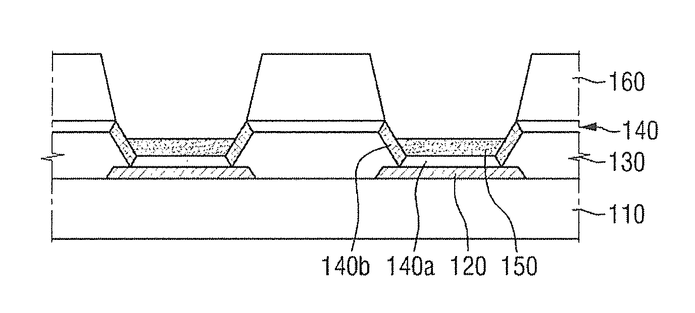
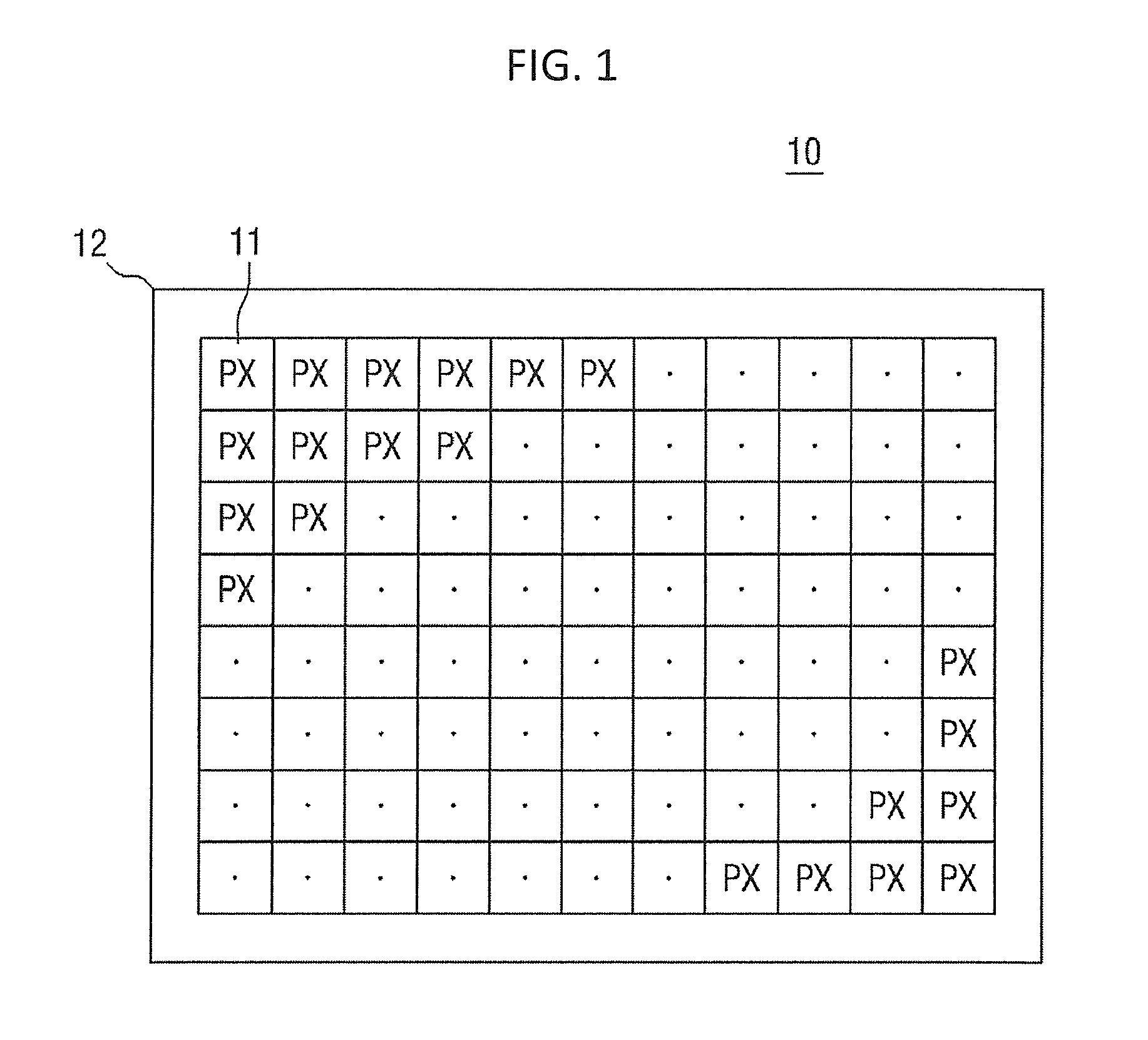
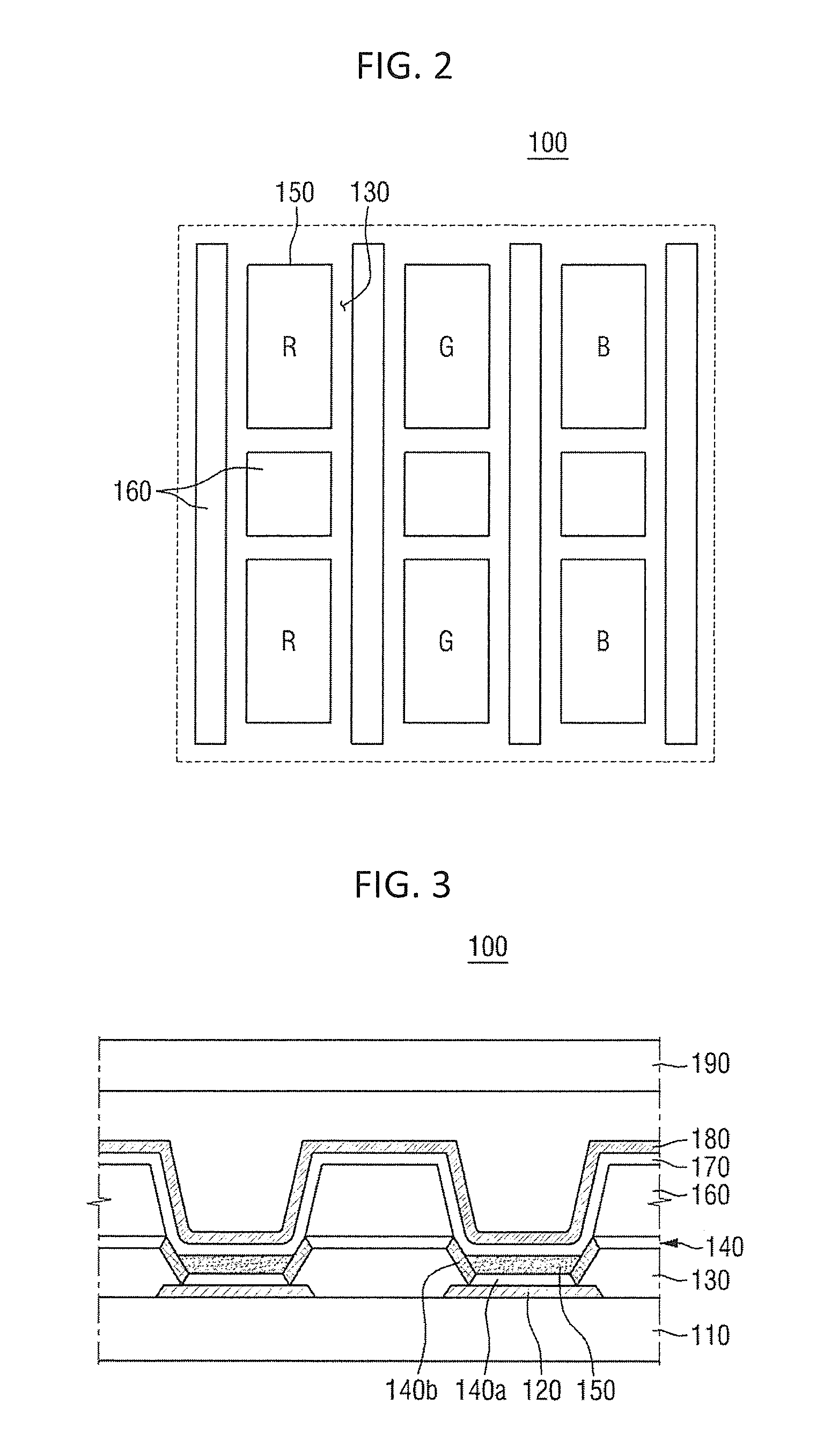
[0008]Aspects of embodiments of the present invention relate to an OLED display and a method of fabricating the OLED display. Further aspects relate to an OLED display including a pixel defining layer and an organic light emission layer, and a method of fabricating the OLED display. Embodiments of the present invention provide for an OLED display that can reduce or prevent dark spots from being caused to pixels due to pressing of a pixel defining layer by forming the pixel defining layer to have a sufficiently large thickness, and can reduce capacitance between lines over and under a pixel defining layer. Further embodiments of the present invention provide for a method of fabricating an OLED display having a pixel defining layer with a sufficiently large thickness. These and other aspects of the present invention will be described in or be apparent to one of ordinary skill in the art from the following description of exemplary embodiments.
[0029]Embodiments of the present invention provide for an OLED display having a pixel defining layer that can be formed to have a sufficiently large thickness to protect the pixels and reduce unwanted capacitance while maintaining film uniformity of a first medium layer. Accordingly, the pixels are not pressed (for example, directly pressed) when an encapsulating substrate is pressed toward the pixels, thereby suppressing dark spots from being generated in the pixels. In addition, as the overall thickness of the pixel defining layer is increased, unwanted capacitance can be reduced or prevented from being generated between electrodes over and under the pixel defining layer.

Problems solved by technology

For example, when an encapsulating substrate is pressed toward pixels in a structure having the encapsulating substrate provided on the organic light emission layer, if the thickness of the pixel defining layer is too small, the pixels may be pressed (for example directly pressed), causing dark spots.
In addition, if the thickness of the pixel defining layer is small, it may cause unwanted capacitance between lines under the pixel defining layer and electrodes over the pixel defining layer.

Method used


Image

  • Organic light emitting diode display and method of fabricating the same
  • Organic light emitting diode display and method of fabricating the same
  • Organic light emitting diode display and method of fabricating the same

Examples


Embodiment Construction

[0038]Aspects and features of the present invention and methods of accomplishing the same may be understood more readily by reference to the following detailed description of exemplary embodiments and the accompanying drawings. The present invention may, however, be embodied in many different forms and should not be construed as being limited to the embodiments set forth herein. Rather, these embodiments are provided to more fully convey concepts of the present invention to those skilled in the art. The scope of the present invention is defined by the appended claims, and their equivalents.

[0039]When an element or layer is referred to as being “on” another element or layer, it can be directly on the other element or layer, or intervening elements or layers may be present. Like numbers refer to like elements throughout. Although the terms first, second, third, etc., may be used herein to describe various elements, components, regions, layers, and / or sections, these elements, componen...


PUM


Abstract

An organic light emitting diode (OLED) display is provided. The OLED display includes: a substrate; a first electrode on the substrate; a first pixel defining layer exposing at least a portion of the first electrode; a medium layer on the first pixel defining layer and the first electrode, the medium layer including a first region and a second region; a second pixel defining layer overlapping the first pixel defining layer with the first region therebetween; a light emission layer overlapping the first electrode with the first region therebetween; and a second electrode covering the second pixel defining layer and the light emission layer.

Description

CROSS-REFERENCE TO RELATED APPLICATION[0001]This application claims priority to and the benefit of Korean Patent Application No. 10-2012-0099777, filed on Sep. 10, 2012 in the Korean Intellectual Property Office, the entire content of which is incorporated herein by reference.BACKGROUND[0002]1. Field[0003]Aspects of embodiments of the present invention relate to an organic light emitting diode (OLED) display and a method of fabricating the same.[0004]2. Description of the Related Art[0005]An OLED display is a self-emissive display device that displays images by exciting an emissive organic material to emit light. The OLED display includes an anode (i.e., a hole injection electrode), a cathode (i.e., an electron injection electrode), and an organic light emission layer interposed therebetween. When the holes and the electrons are injected into the light emission layer, they recombine to form excitons, which emit light when they change from an excited state to a ground state.[0006]The...

Claims


Application Information

Patent Timeline
Patent Type & Authority Patents(United States)
IPC IPC(8): H01L51/52H01L51/56H01L27/32
CPCH01L51/52H01L27/3246H01L51/56H10K59/122H01L21/02288H01L21/67051H01L2224/95134H10K2102/351H10K50/80H10K71/00
Inventor KANG, JIN GOO
Owner SAMSUNG DISPLAY CO LTD
Why Eureka
Try Eureka