Supercharge Your Innovation With Domain-Expert AI Agents!

Method for forming laminate and laminating device

a technology of laminating device and laminate, which is applied in the direction of presses, other domestic objects, manufacturing tools, etc., can solve the problems of uneven thickness of adhesive sheet, inability to maintain the parallelism of compressing surface itself of both press plates, and inability to maintain the flat surface of adhesive sh

Active Publication Date: 2015-04-14
THE JAPAN STEEL WORKS LTD
View PDF17 Cites 0 Cited by
  • Summary
  • Abstract
  • Description
  • Claims
  • Application Information

AI Technical Summary

Benefits of technology

This approach ensures a uniform thickness of the laminate with complete penetration of the projection through the film-shaped laminating body, preventing deformation and voids, and maintaining consistent contact pressure, even with non-parallel surfaces, thus enhancing the lamination process.

Problems solved by technology

H11-4076, in the case of using the planar press machine, there have been problems such as not being able to form the film-shaped laminating body to be laminated on the laminate base body with a uniform thickness, the projection such as the bump being crushed by partially being compressed excessively, the film-shaped laminating body becoming thinner than a designed thickness, raising from a reason that a mechanical parallelism for maintaining both press plates parallel cannot be maintained accurately, or that a parallelism of compressing surfaces themselves of both of the press plates cannot be maintained accurately.
Further, in JP-A No. 2009-32853, since the semiconductor wafer and the ring frame are mounted on the supporting unit, the adhesive sheet is positioned above them, and the adhesive sheet is pressed against the semiconductor wafer and the ring frame by the adhesive sheet being sandwiched, a surface of the adhesive sheet does not become flat, and a thickness thereof does not become uniform.
In JP-A No. 2005-150273, since a core substrate and a prepreg sheet are compressed between the upper plate and the bottom portion of the container chamber via the pair or rubber-made pressing members, the prepreg sheet cannot be laminated with a uniform thickness due to not being able to ensure a parallelism, similar to both of the press plates of the planar press machine of JP-A No.
Further, since the compression is performed by the rubber-made pressing member merely by vacuum suction, there may be cases in which a sufficient compression force cannot be ensured.

Method used


Image

  • Method for forming laminate and laminating device
  • Method for forming laminate and laminating device
  • Method for forming laminate and laminating device

Examples


Embodiment Construction

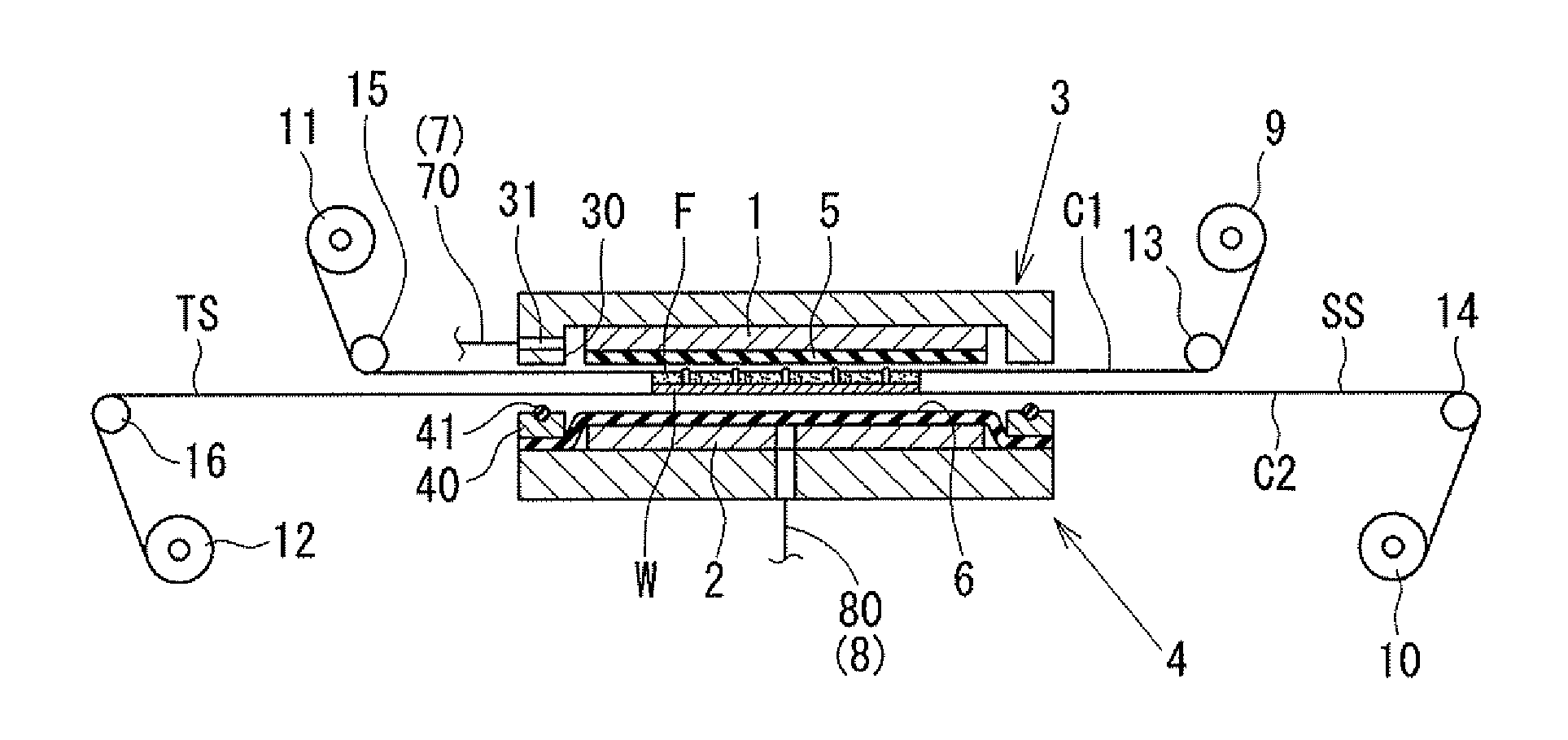
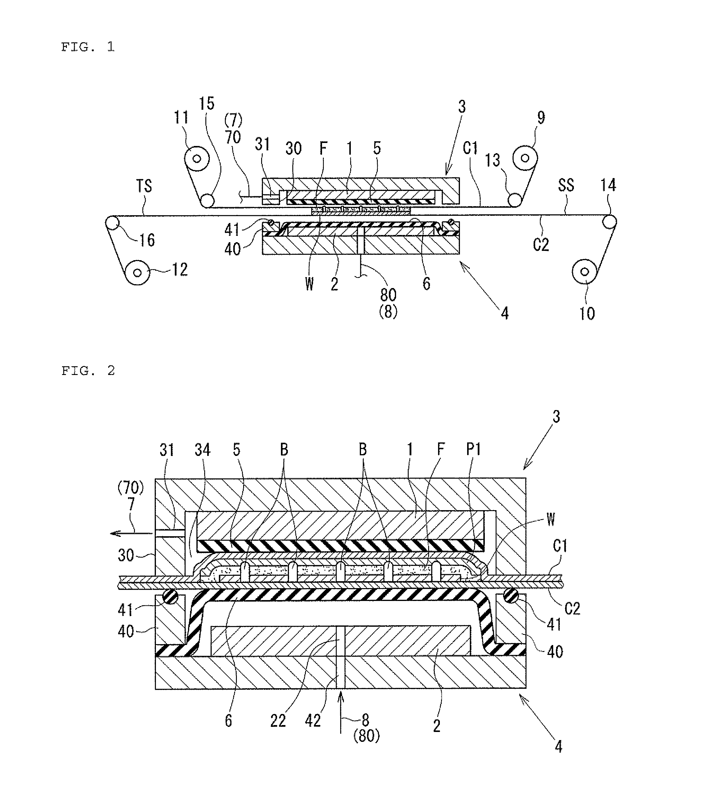
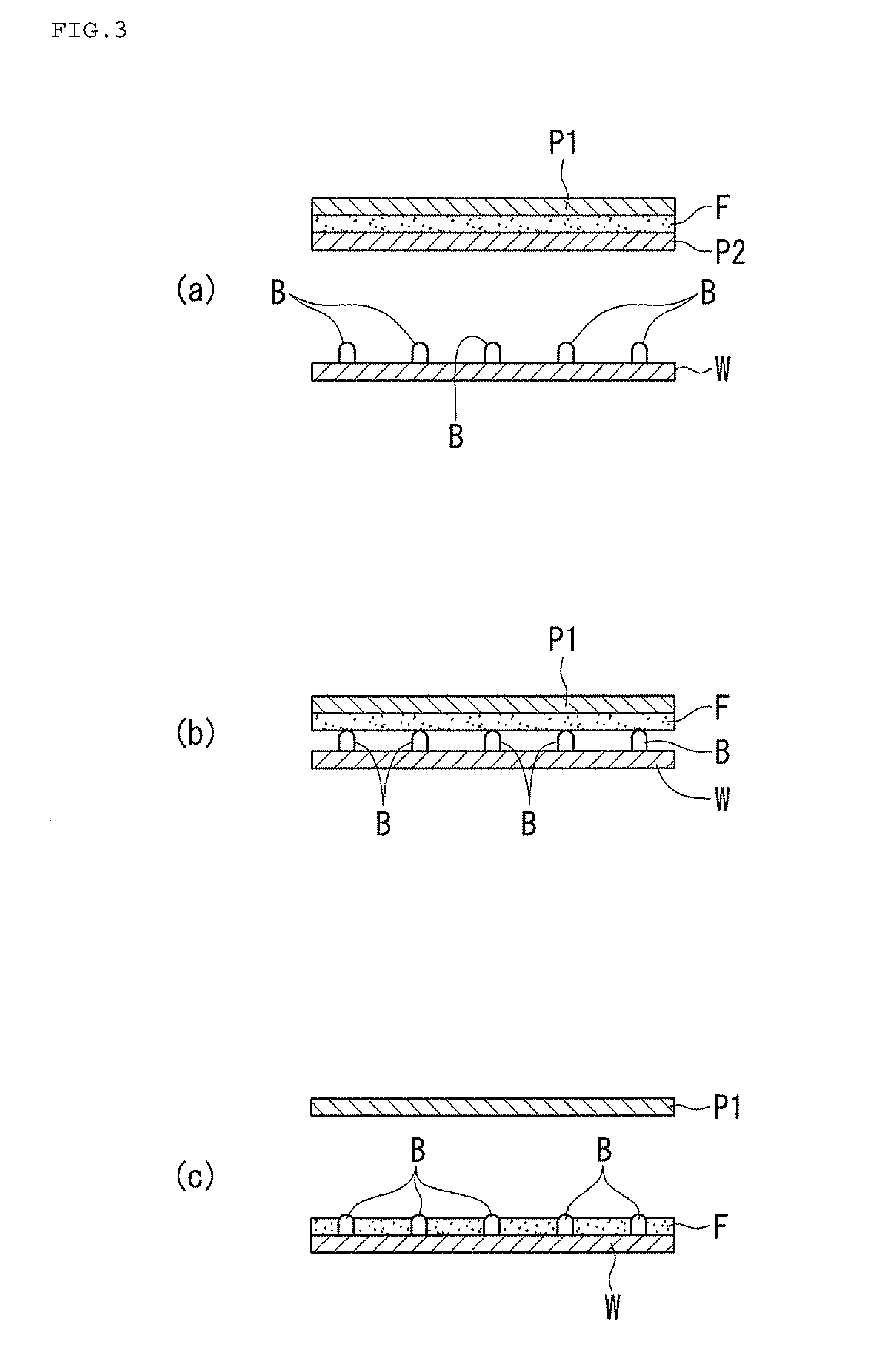
[0038]Firstly, an embodiment of a laminating device of the present invention will be described in detail with reference to FIG. 1 and FIG. 2. Note that, in this embodiment, explanations will be given for a case in which a laminate base body including a projection is a semiconductor wafer W including bumps B (hereinafter, the projection is referred to as the bump, and the laminate base body is referred to as the semiconductor wafer), and a film-shaped laminating body is an insulating resin film (hereinafter, the film-shaped laminating body is referred to as the insulating resin film) F that at least has a protection film P1 disposed on a surface opposite from a surface that is to be laminated upon forming a laminate with the semiconductor wafer W as shown in FIG. 3.

[0039]Schematically, the laminating device of the present invention is for forming a laminate by layering the semiconductor wafer W including the bumps B and the insulating resin film F, and heating and compressing the sam...


PUM

PropertyMeasurementUnit
diameteraaaaaaaaaa
thicknessaaaaaaaaaa
diametersaaaaaaaaaa

Abstract

A surface of a laminate base body including a projection is caused to penetrate at least a film-shaped laminating body and surely laminated by a simple configuration, and a laminate thereof is formed at a uniform thickness without an occurrence of voids. A laminating device is provided with a heating unit configured to heat at least an insulating resin film; an upper plate and a lower plate configured to be capable of opening and closing, and configured to form a chamber that becomes sealed upon closing; a receiving member having an elasticity and disposed on the upper plate; an elastic membrane body disposed on the lower plate; a vacuuming unit configured to vacuum inside of the chamber; and a compressing unit configured to bloat the elastic membrane body.

Description

BACKGROUND OF THE INVENTION[0001]1. Field of the Invention[0002]The present invention relates to a method for forming a laminate and a laminating device, and especially relates to a method for forming a laminate by layering a laminate base body including a projection, such as an electronic component including bumps, and a film-shaped laminating body, such as a resin, and heating and compressing the same so that the projection penetrates at least the film-shaped laminating body, and a device therefor.[0003]2. Description of the Related Art[0004]As a laminate base body such as an electronic component including a projection, for example, on a surface of a semiconductor wafer, bumps made of metal such as solder, copper, and gold is formed. These bumps project from the surface of the semiconductor wafer, typically are formed in a columnar shape with a tip resembling a sphere, or an egg shape, and have a height (projection amount) about 0.01 to 0.04 mm and a diameter about 0.01 to 0.04 mm...

Claims


Application Information

Patent Timeline
Patent Type & Authority Patents(United States)
IPC IPC(8): B29C65/00B32B37/00B32B37/10B32B37/14
CPCB32B37/14B32B37/10B32B37/1009B32B2457/14H01L2224/75315H01L2224/75317Y10T156/1002
Inventor HIROSE, TOMOAKIYAMAMOTO, TAKAYUKI
Owner THE JAPAN STEEL WORKS LTD
Features
  • R&D
  • Intellectual Property
  • Life Sciences
  • Materials
  • Tech Scout
  • Unparalleled Data Quality
  • Higher Quality Content
  • 60% Fewer Hallucinations
Learn More