

Electrooptic device, method for driving electrooptic device and electronic apparatus
a technology of electrooptic devices and electronic devices, applied in the direction of instruments, light sources, computing, etc., can solve the problems of degrading display quality, and achieve the effect of simplifying and reducing the size of an electrooptic device, and not degrading display quality
- Summary
- Abstract
- Description
- Claims
- Application Information
AI Technical Summary
Benefits of technology
Problems solved by technology
Method used
Image

Examples
first embodiment
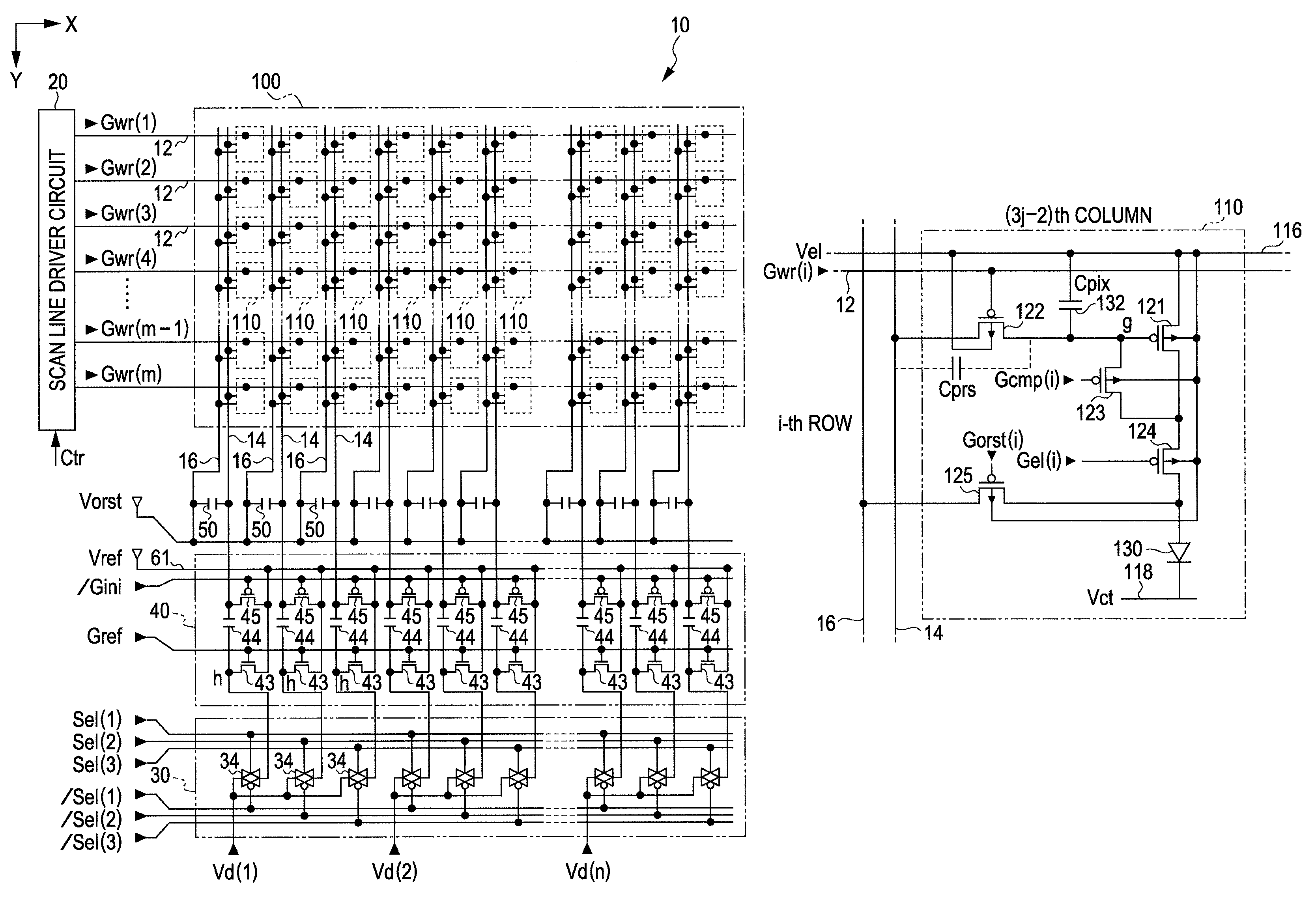
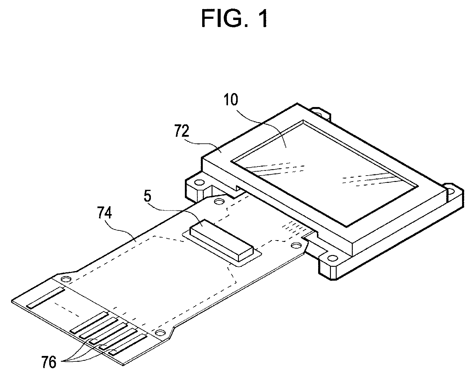
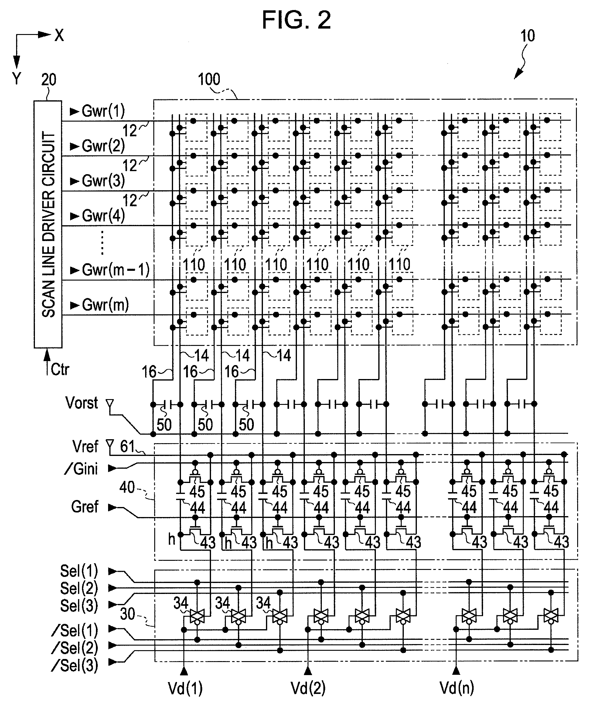
[0056]FIG. 1 is a perspective view which shows a structure of an electrooptic device 10 of an embodiment of the invention.
[0057]The electrooptic device 10 is a micro-display which displays an image, e.g., in a head mounted display. The electrooptic device 10 is an organic EL device in which a plurality of pixel circuits, driving circuits which drive the pixel circuits, etc., are formed, e.g., on a silicon substrate as described later in detail, and an exemplary light emitting element, an OLED, is used for the pixel circuit. The electrooptic device 10 is contained, e.g., in a frame-like case 72 which is open on a display section, and is connected with one end of an FPC (Flexible Printed Circuits) board 74. A control circuit 5 in a semiconductor chip is mounted on the FPC board 74 by means of COF (Chip On Film) technology, and the FPC board 74 is provided with a plurality of terminals 76 and is connected with an upper rank circuit which is omitted to be shown. The upper rank circuit p...
second embodiment
Operation of Second Embodiment
[0154]An operation of the electrooptic device 10 of the second embodiment will be explained with reference to FIG. 12. FIG. 12 is a timing chart for explaining an operation of the second embodiment.
[0155]As shown in the drawing, the second embodiment works in the same way as the first embodiment in that the scan signals Gwr(1)-Gwr(m) are changed to L level in turn and the scan lines 12 of the first to m-th rows are scanned in turn over a period of time for one frame in every period for horizontal scanning (H). Further, the second embodiment works in the same way as the first embodiment as well in that the period for scanning the i-th row is formed by the periods of initialization, compensation and writing indicated with (b), (c) and (d), respectively, in this order. Incidentally, the period for writing (d) is a period of time since the control signal Gcp1 changes from L to H level (the control signal / Gcp1 changes to L level) until the scan signal chang...
examples of application and modification
[0195]The invention is not limited to embodiments and so on such as the embodiments described above or application examples, and can be variously modified as described below. Further, any one or a plurality of modifications described below can be suitably combined with one another.
[0196]Control Circuit
[0197]Although it is supposed as to the embodiment that the control circuit 5 which provides a data signal is separate from the electrooptic device 10, the control circuit 5 may be integrated with the scan line driver circuit 20, the demultiplexer 30 and the level shift circuit 40 on the silicon substrate.
[0198]Further, the electrooptic device 10 may include the control circuit 5. In this case, the electrooptic device 10 has a driver circuit which drives the pixel circuit 110 and the driver circuit is provided with a driving control circuit which controls operations of the pixel circuit 110, the demultiplexer 30 and the level shift circuit 40.
[0199]Substrate
[0200]Although being structu...
PUM
 Abstract
Description
Claims
Application Information