Low-cost electrostatic discharge (ESD) protection device for high-voltage open-drain pad
- Summary
- Abstract
- Description
- Claims
- Application Information
AI Technical Summary
Benefits of technology
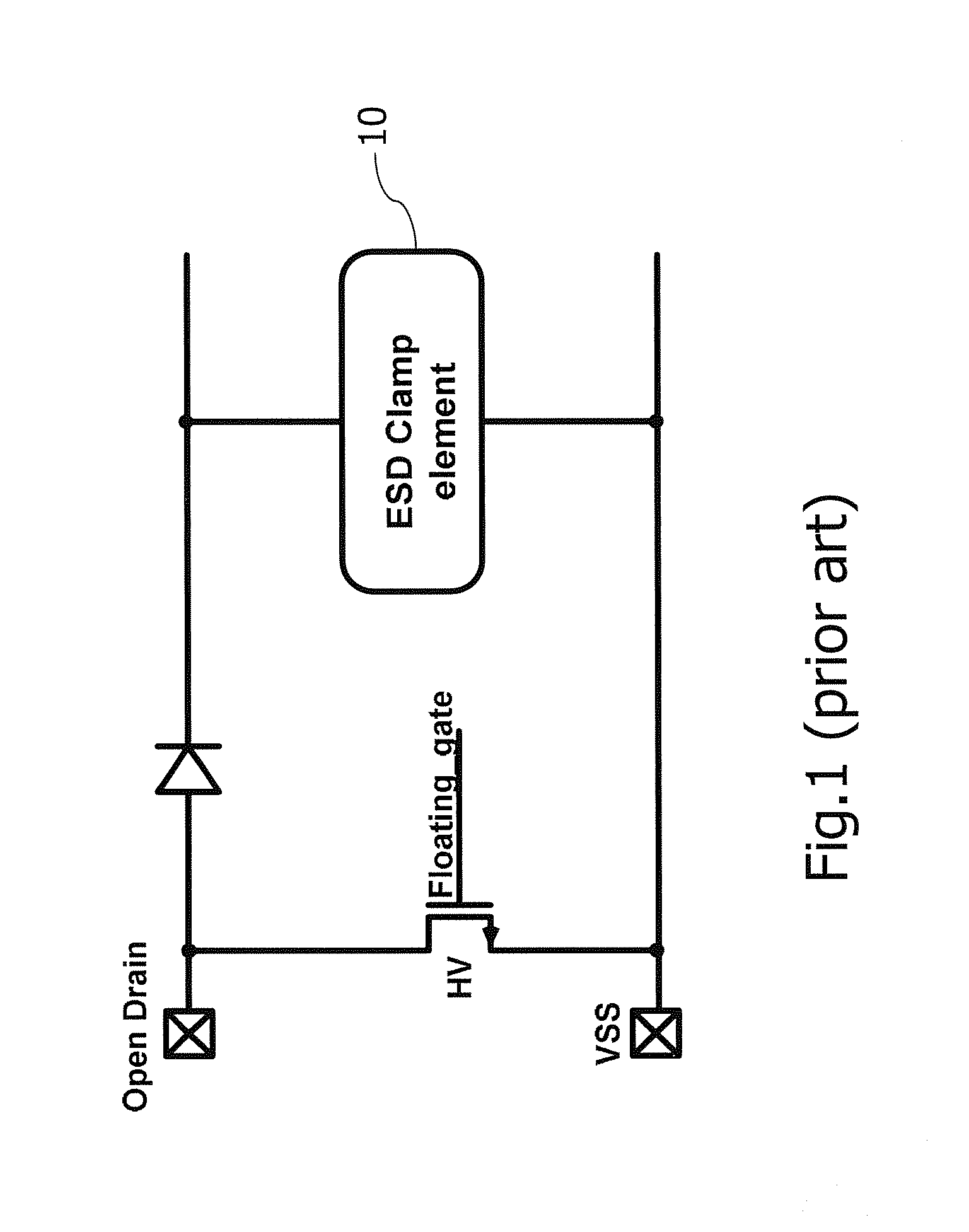
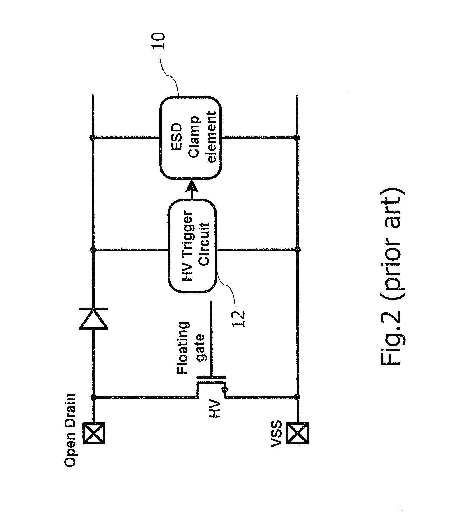
Problems solved by technology
Method used
Image
Examples
Embodiment Construction
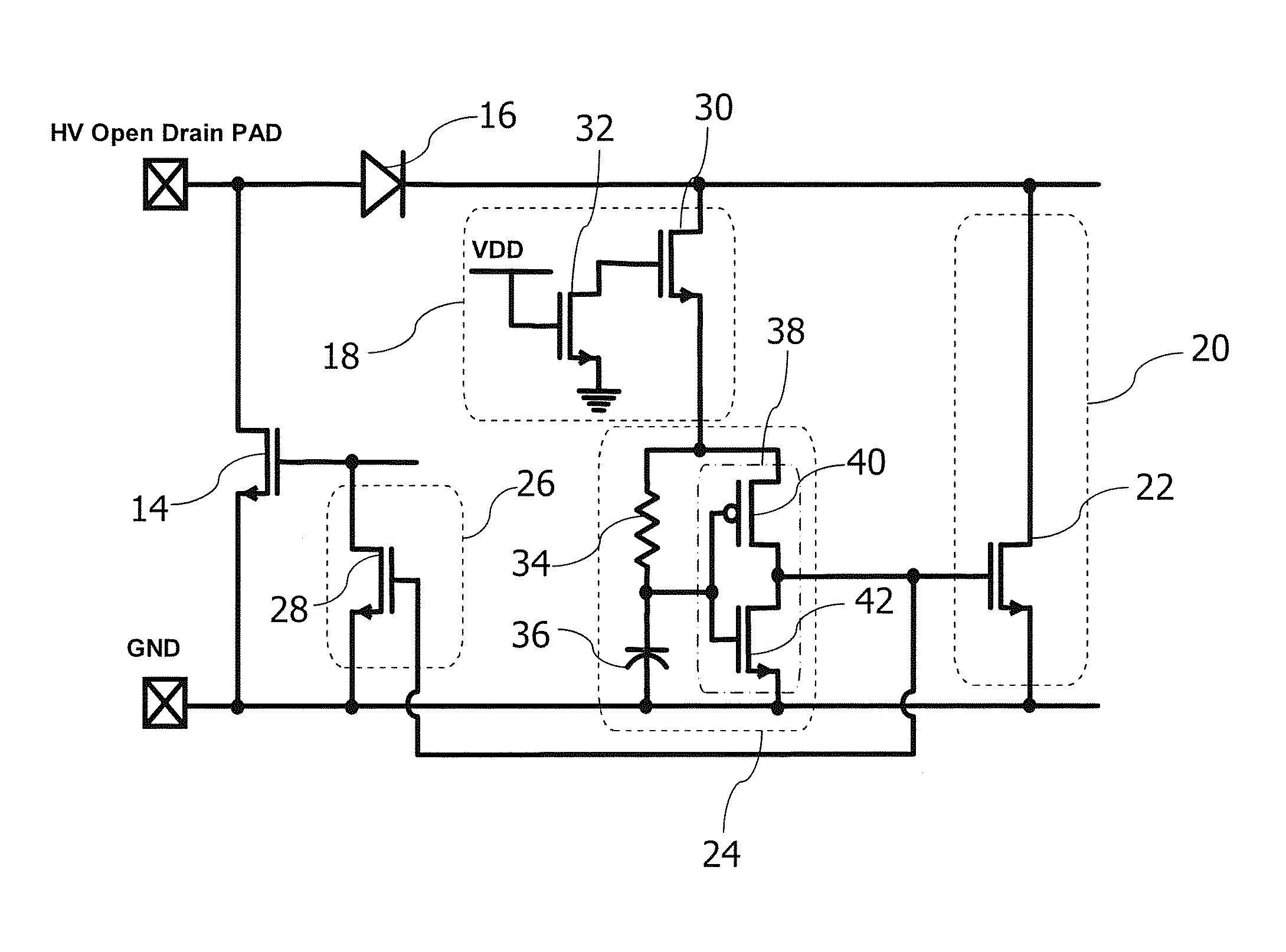
[0014]Refer to FIG. 3. The first embodiment of the present invention is described as below. The present invention comprises a first high-voltage
[0015]N-channel metal oxide semiconductor field effect transistor (HV NMOSFET) 14 coupled to a high-voltage (HV) open drain pad and a low-voltage (LV) ground pad GND. In normal operation, a driving circuit coupled to a gate of the first HV NMOSFET 14 can turn on or off the first HV NMOSFET 14, so that the first HV NMOSFET 14 receives a high voltage on the HV open drain pad to operate. When an ESD event is applied to the HV open drain pad, the gate of the first HV NMOSFET 14 is turned off by a LV bias unit 26. An anode of a diode 16 is coupled to the HV open drain pad and the first HV NMOSFET 14, and a cathode of the diode 16 is coupled to a high-voltage (HV) block unit 18 and an electrostatic discharge (ESD) clamp unit 20, wherein the ESD clamp unit is exemplified by a high-voltage N-channel metal oxide semiconductor field effect transistor ...
PUM
 Abstract
Description
Claims
Application Information


