Optical sensor device

a sensor device and optical sensor technology, applied in the direction of optical radiation measurement, radiation control devices, semiconductor/solid-state device details, etc., can solve the problems of low thermal resistance of resins, and low environmental reliability, so as to improve thermal resistance and thermal resistance, the difference in the coefficient of expansion can be extremely reduced, and the stability of electrical continuity and high reliability against environmental chang

Inactive Publication Date: 2015-05-12
ABLIC INC
View PDF8 Cites 13 Cited by
  • Summary
  • Abstract
  • Description
  • Claims
  • Application Information

AI Technical Summary

Benefits of technology

[0022]The optical sensor device according to the present invention can completely hermetically seal the optical sensor element with glass. The metal is ill led in the through-electrode, and the filled metal also forms the wiring patterns provided on the front surface and the rear surface of the glass substrate having a cavity so as to be integral therewith. This not only causes the element to be free from stress but also stabilizes electrical connection between the front surface and the rear surface of the glass substrate having a cavity and prevents the through-electrode and the wiring patterns from easily separating from each other, and thus, obtains high reliability in mounting. Further, the wiring patterns provided by metalization on the front surface of the glass substrate having a filter function and the front surface of the glass substrate having a cavity are fixed to each other and, at the same time, electrically connected to each other by the adhesive having conductive particles added thereto, and thus, a package which has both stability in electrical continuity and high reliability against environmental change is obtained. Further, the package has a structure in which glass substrates are bonded together and which includes only a glass material, and thus, the difference in coefficient of expansion can be extremely reduced, and an optical sensor device which is excellent in cost, properties, reliability in mounting, and reliability can be provided.

Problems solved by technology

At the same time, in the fiat screen televisions, and the inside end outside lighting devices, there has been a development problem of an energy-saving rate along with an increase in performance year after year, and many of the televisions and devices have a function of controlling the illuminance finely.
However, the optical sensor device described in Japanese Published Patent Application No. 2007-36264 has a package structure in which an epoxy resin or the like is used for sealing the element, and hence has a problem such as weak in environmental reliability including heat resistance and moisture resistance of the material.
Further, the resin used for sealing the element is required to be translucent, and thus, it is generally thought to be difficult for the resin to be resistant to heat at the same time.
It follows that the range of selection of the sealing resin which significantly determines the reliability of the device is limited: low resistance to heat; low stress; easy to take up moisture; easy to expand at a high temperature; and the like.
As a result, it is difficult to obtain high performance in an environment in which heat and moisture are added or in an environment in which expansion and contraction are repeated in a temperature cycle repeating high temperature and low temperature as in a reliability test.
It is known that, as a result, the sealing resin is gradually deteriorated and exhibits discoloration or the like, and at the same time, the transmittance thereof is lowered.
As a result, there is a problem that light is less liable to enter the optical sensor element, and desired properties and reliability as art optical sensor device cannot be obtained.
As a result, for example, in reflowing carried out in a process of mounting the optical sensor device, phenomena such as wicking and erosion of solder paste used for connection to the mounted substrate are accompanied by entry of the solder paste from between the sealing resin and the electrode 4, and a risk of separation of the wire or separation from the sealing resin increases.
This improvement obtains the effect of improving performance in an environment in which expansion and contraction are repeated in a temperature cycle repeating high temperature and low temperature, which causes a problem of a conventional sealing resin material.
The optical sensor device described in Japanese Published Patent Application No. 2007-234783 obtains the effect by containing an inorganic filler in a transparent epoxy resin or the like for sealing, but, when an inorganic filler is mixed in a resin, it is known that air exists at an interface between the inorganic filler and the resin a rut that it is not easy to mix the inorganic filler in the resin so that the refractive index and the surface state of the inorganic filler do not lower the optical properties of the transparent sealing resin at all.
Accordingly there is a possibility that the effect of improving the reliability of the optical sensor device by adding inorganic filler is limited.
Further, the optical sensor device described in Japanese Published Patent Application No. 2007-234783 has the lead portion 22 for external connection of the leadframe 20, the lead portion 22 being relatively away from the optical sensor element 10 and protruding significantly from the sealing resin 30, and thus, the reliability in mounting is improved, but the package size is liable to increase, and it is difficult to enjoy the merits of miniaturization.
Accordingly, it is difficult to accommodate the use where portability is required.

Method used


Image

  • Optical sensor device
  • Optical sensor device
  • Optical sensor device

Examples


first embodiment

[0035]The structure of an optical sensor device according to this embodiment is hereinafter described with reference to the drawings.

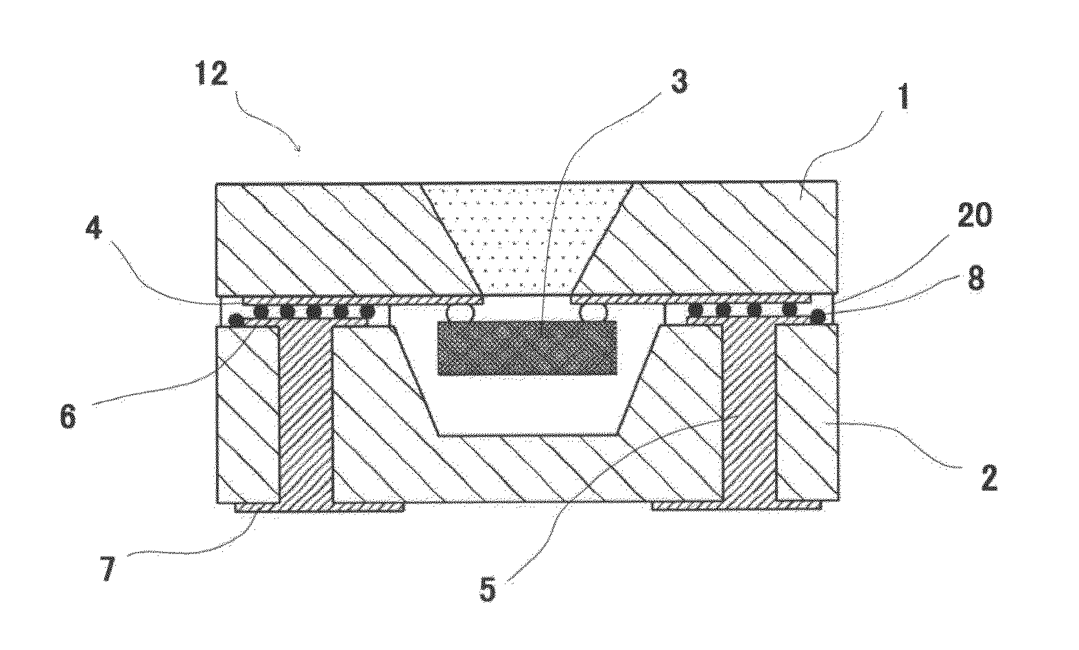
[0036]FIG. 1 is a schematic view illustrating an optical sensor device 12 according to this embodiment. FIG. 1 is a longitudinal cross-sectional view of the optical sensor device 12. The optical sensor element 3 is mounted on the glass lid substrate 1 having a filter function. The glass lid substrate 1 is bonded to the glass substrate 2 having a cavity (glass substrate with a cavity) to be integral therewith. The wiring pattern 4 is formed by metalization on the bottom surface of the glass lid substrate 1 and, as illustrated, does not extend inside the glass lid substrate. The optical sensor element 3 is mounted in the center of the glass lid substrate 1 and is electrically connected to the wiring pattern 4. The optical sensor element 3 is mounted on and electrically connected to the wiring pattern 4 provided by metalization on the glass lid substrate ...

second embodiment

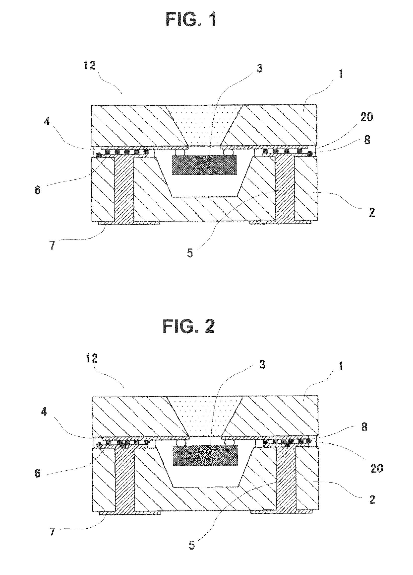
[0040]FIG. 2 is a cross-sectional view of the optical, sensor device 12 according to this embodiment. The structure of being bonded to the glass lid substrate 1 is similar to that of the first embodiment, but the wiring pattern provided by metalization on the front surface of the glass substrate 2 is partially concave. When the glass lid substrate 1 and the glass substrate 2 are bonded and fixed to each other, the wiring pattern 4 provided by metalization on the glass lid substrate 1 and the wiring pattern 6 provided by metalization on the front surface of the glass substrate having a cavity are fixed to each other with the adhesive 20 having conductive particles added, thereto. By providing a concave portion in the bonded location in a part of the wiring pattern provided on the glass substrate 2, the thickness of the adhesive may be set partially large.

[0041]Further, since the conductive particles which carry out electrical connection build up in the concave portion, a plurality of...

third embodiment

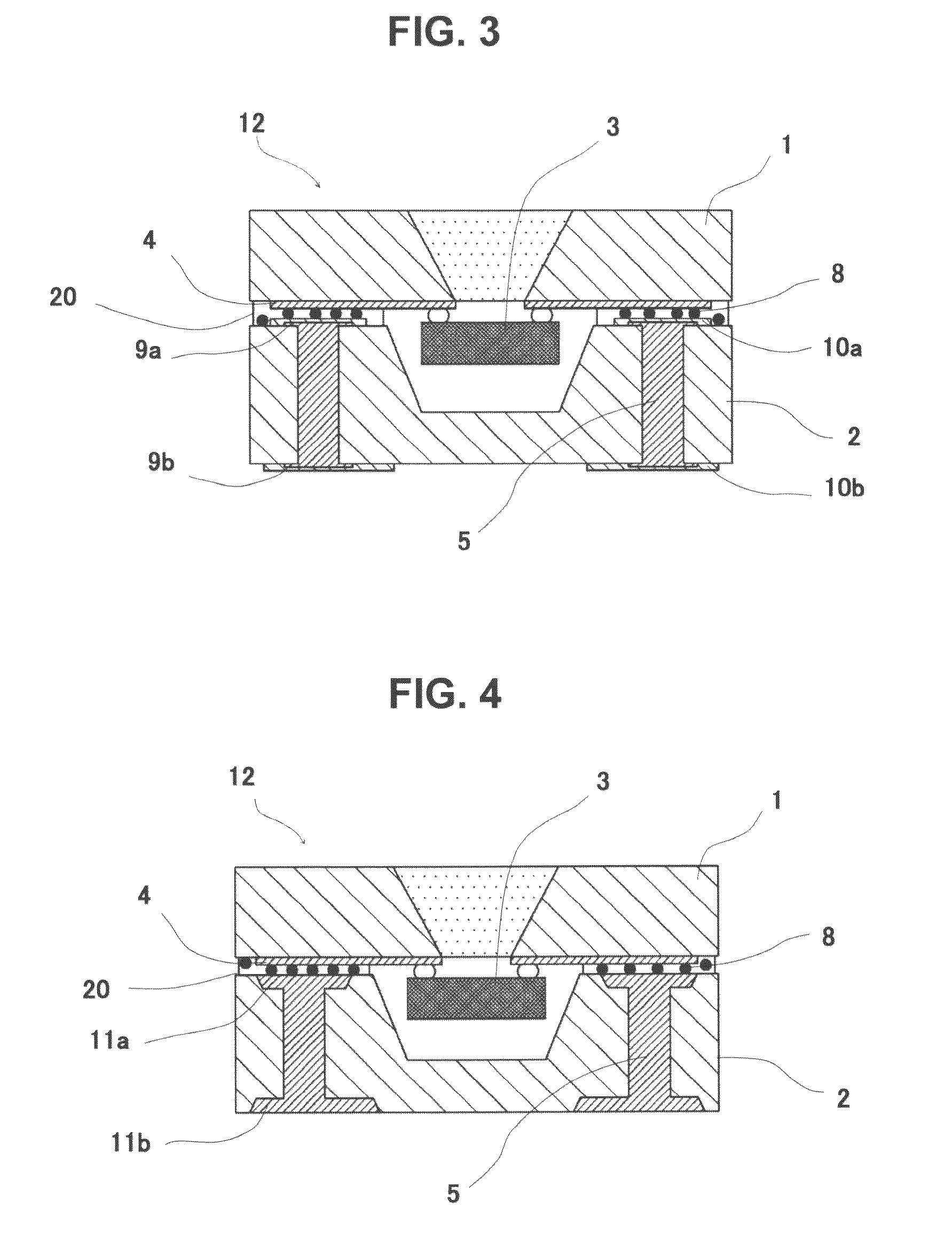
[0042]FIG. 3 is a cross-sectional view of the optical sensor device 12 according to this embodiment. The through hole which is provided in the glass substrate 2 and in which metal is filled in the first embodiment is formed using, for example a metal pin. A part of the metal pin is exposed on the front surface and the rear surface of the glass substrate 2, and the exposed portions have thin and flat shapes 9a and 9b, respectively. A part of the exposed pin also serves as a wiring pattern. Further, a part of the pin exposed on the front surface and the rear surface of the glass substrate 2 may additionally have wiring patterns 10a and 10b provided by metalization on the surfaces thereof. The wiring patterns are formed by metalization on the metal surfaces of the pin, and thus, the metal which forms the wiring patterns diffuses toward surface layers of the pin and can have firm coupling. This effect enables the metal pin and the wiring patterns provided by metalization to have a so-ca...


PUM


Abstract

An optical sensor element is mounted in a package which includes a glass substrate having a cavity, and a glass lid substrate bonded to the other substrate to close the cavity. The glass substrate with the cavity has metalized wiring patterns on front and rear surfaces thereof, and a through hole filled with metal to form a through-electrode interconnecting the wiring patterns on the front and rear surfaces. A metalized wiring pattern on the rear surface of the glass lid substrate is electrically connected to the wiring pattern on the front surface of the other substrate with an adhesive containing conductive particles. The glass lid substrate is made either of glass having a filter function or glass having a light shielding property with an opening therethrough filled with glass having a filter function.

Description

BACKGROUND OF THE INVENTION[0001]1. Field of the Invention[0002]The present invention relates to an optical sensor device in which an optical sensor element is mounted on a package material using a glass substrate.[0003]2. Description of the Related Art[0004]In recent years, mobile terminals such as mobile personal computers, tablet personal computers, and smartphones are rapidly becoming widespread. Further, flat screen televisions and LED lighting for inside and outside lighting devices are significantly becoming widespread. The reason behind this is because those mobile terminals have a large number of functions and another main reason is that they are designed to promote portability such as light in weight and thin in thickness. At the same time, in the fiat screen televisions, and the inside end outside lighting devices, there has been a development problem of an energy-saving rate along with an increase in performance year after year, and many of the televisions and devices ha...

Claims


Application Information

Patent Timeline
Patent Type & Authority Patents(United States)
IPC IPC(8): H01L31/0232G01J1/02G01J1/42G01J1/44
CPCG01J1/44G01J1/0271G01J1/0204G01J1/42
Inventor TSUKAGOSHI, KOJIKAMAMORI, HITOSHIOKU, SADAOFUJITA, HIROYUKIHAYASHI, KEIICHIRO
Owner ABLIC INC
Why Eureka
Try Eureka