
Multi-level cell operation in silver/amorphous silicon RRAM

a technology of amorphous silicon and multi-level cells, applied in information storage, static storage, digital storage, etc., can solve the problems of a bit line and a capacitive discharge of a word line that interfere with cell programming, and achieve the effect of facilitating more than one resistance sta

Active Publication Date: 2015-06-16
CROSSBAR INC
View PDF86 Cites 1 Cited by
  • Summary
  • Abstract
  • Description
  • Claims
  • Application Information

AI Technical Summary

Benefits of technology

The present invention provides a method for programming a resistive switching device by applying a forward bias voltage to cause it to be in a low resistance state or programmed state. This method allows for a multi-level cell with more than one resistance states or erased states and a multi-bit device. As conventional methods use different forward bias voltages for forming a multi-bit device, capacitive discharge from a word line and a bit line interferes with programming of a cell. However, the present method eliminates this interference and allows for well-controlled multi-level cells to be realized.

Problems solved by technology

As conventional method uses different forward bias voltages to form a multi-bit device, capacitive discharge from a word line and a bit line interferes with programming of a cell.

Method used


Image

  • Multi-level cell operation in silver/amorphous silicon RRAM
  • Multi-level cell operation in silver/amorphous silicon RRAM
  • Multi-level cell operation in silver/amorphous silicon RRAM

Examples


Embodiment Construction

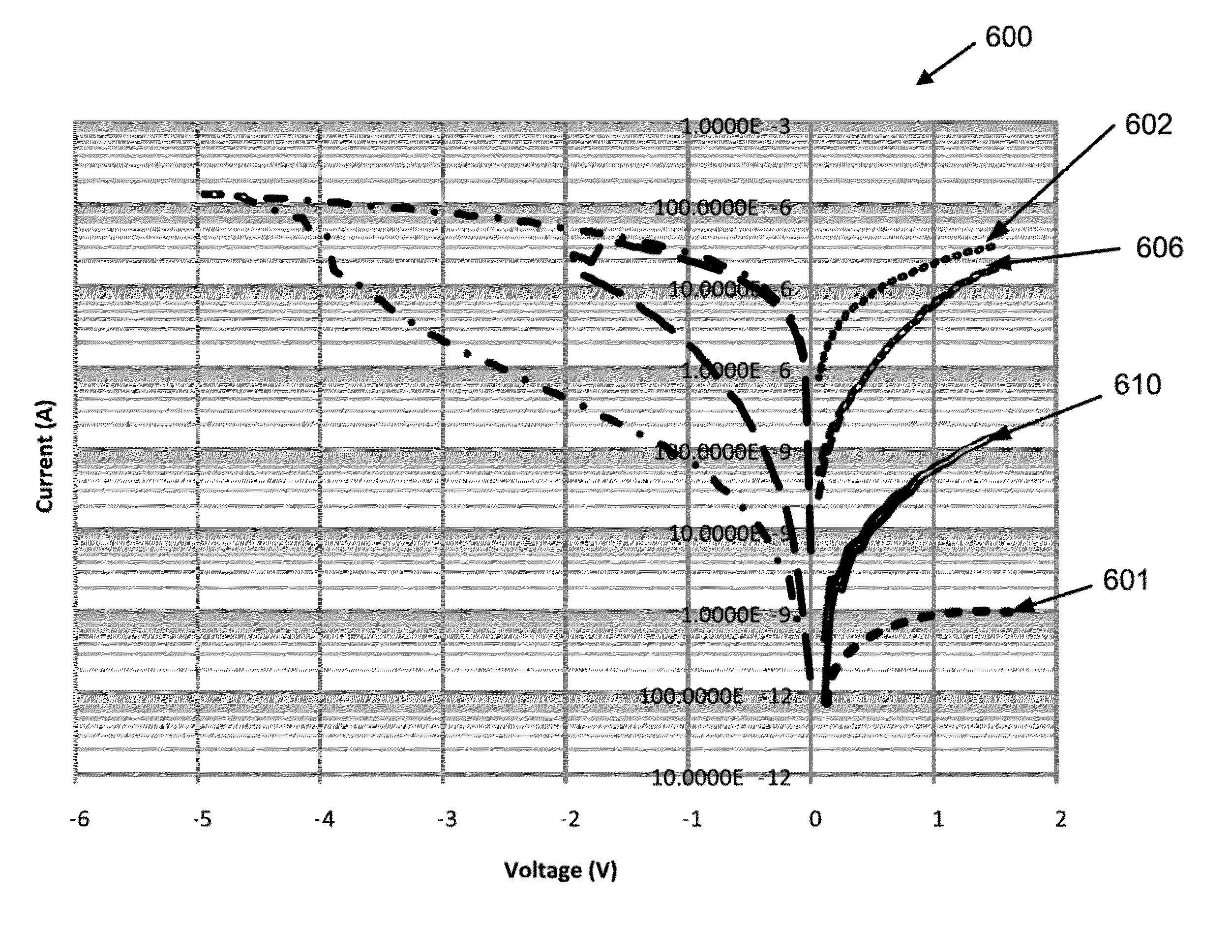
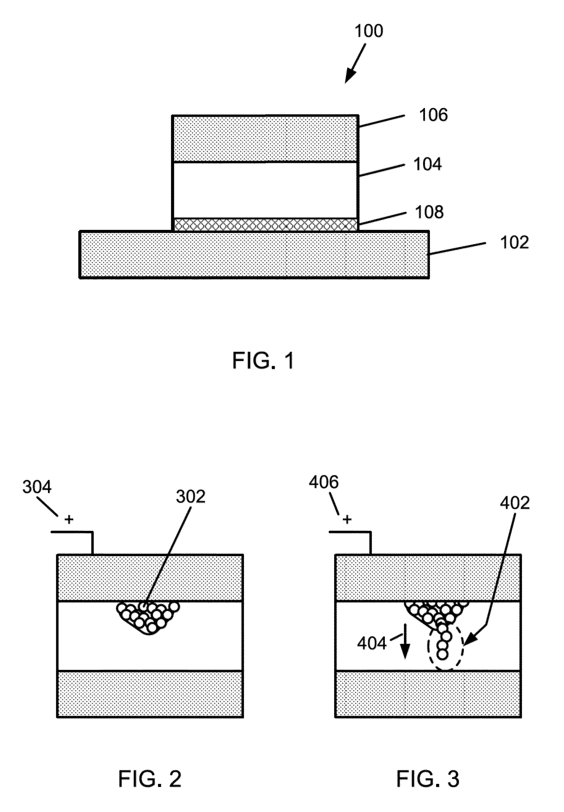
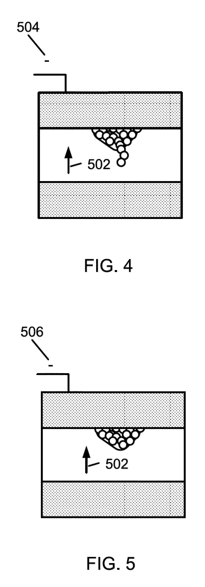
[0018]The present invention is generally related to resistive switching devices. More particularly, embodiments according to the present invention provide a programming method for a multi-level cell. Embodiments of the present invention have been applied to non-volatile memory devices using silver as a conductor material and an amorphous silicon material as a switching material, but it should be recognized that the present invention can have a much broader range of applicability.

[0019]A resistive switching device based on silver / amorphous silicon has the potential to have a multi bit operation. But current control during programming to obtain different states in the cell is difficult to facilitate especially for a far-far bit. This is due to capacitive discharge from a distributed capacitance and resistance from both a bitline and a wordline. Embodiments according to the present invention use a programmed (or written) cell and one or more erase operations to provide a well-controlle...


PUM


Abstract

A method of programming a non-volatile memory device includes providing a resistive switching device, the resistive switching device being in a first state and characterized by at least a first resistance, applying a first voltage to the resistive switching device in the first state to cause the resistive switching device to change to a second state wherein the second state is characterized by at least a second resistance, wherein the second resistance is greater than the first resistance, and applying a second voltage to the resistive switching device in the second state to cause the resistive switching device to change to a third state, wherein the third state is characterized by at least a third resistance, wherein the second voltage has a magnitude higher than a magnitude of the second voltage, and wherein the third resistance is greater than the second resistance.

Description

CROSS REFERENCE TO RELATED APPLICATIONS[0001]The subject application for patent claims priority to U.S. provisional patent application No. 61 / 503,447 filed on Jun. 30, 2011.STATEMENT RELATED TO GOVERNMENT OR FEDERALLY FUNDED RESEARCH[0002]Not ApplicableBACKGROUND[0003]The inventors of the present invention have recognized the success of semiconductor devices has been mainly driven by an intensive transistor down-scaling process. However, as field effect transistors (FETs) approach sizes less than 100 nm, physical problems such as short channel effect begin to hinder proper device operation. For transistor based memories, such as those commonly known as Flash memories, other performance degradations or problems may occur as device sizes shrink. With Flash memories, a high voltage is usually required for programming of such memories. However, as device sizes shrink, the high programming voltage can result in dielectric breakdown and other problems. Similar problems can occur with othe...

Claims


Application Information

Patent Timeline
IPC IPC(8): G11C13/00
CPCG11C13/00G11C11/56G11C11/5614G11C13/0002G11C13/0009G11C13/0011G11C13/0069G11C2013/0083G11C2213/33
Inventor JO, SUNG HYUNKUMAR, TANMAY
Owner CROSSBAR INC
Learn More