
Vacuum photosensor device with electron lensing

a photosensor and vacuum technology, applied in the field of vacuum sealed photosensor devices, can solve the problems of insufficiently large-scale production of large-area photosensors, low quality, labor-intensive, etc., and achieve the effects of reducing production costs, reducing production costs, and improving production efficiency

Active Publication Date: 2015-06-23
RGT UNIV OF CALIFORNIA
View PDF10 Cites 1 Cited by
  • Summary
  • Abstract
  • Description
  • Claims
  • Application Information

AI Technical Summary

Benefits of technology

[0019]The individual elements (pixels) of the present invention may be seamlessly combined into a flat-panel array that provides for light detection without dead areas which fail to collect and register light between the sensing pixels.
[0020]In one embodiment, a vacuum-enclosing portion of the device comprises three inexpensive, mass-produced glass elements: a vacuum housing (e.g., hemisphere), a base plate and a central electron readout element. This allows for scalable mass production with low investment. When constructed of ultrapure quartz, the inventive photosensor provides an unprecedented low level of radioactivity. In one embodiment, a thin-film deposited sealing means retains the ultra-high vacuum while also serving as high voltage throughputs, eliminating any need for electrodes or solid metallic feedthroughs.
[0021]The present invention provides a readily fabricated, highly sensitive, universal and durable photosensor solution which is scalable as it does not rely on the production of large monolithic sensor panels. The present invention also provides for scalable industrial mass production which is achievable at a fraction of the cost required when producing classical photomultipliers, classical hybrid photon diodes (HPD), as well as large area monolithic flat-panel devices, including those described in U.S. Pat. No. 6,674,063 which is incorporated herein by reference in its entirety, and those described in PCT International Publication No. WO 2007 / 098493 A2 published on Aug. 30, 2007 which is incorporated herein by reference in its entirety. It will be appreciated that the cost of facilities for fabricating a UHV device increases steeply as a function of physical size.
[0022]Accordingly, an aspect of the invention is a vacuum photosensor device which provides high collection rate and accurate measurements within a robust structure which can be readily mass produced.
[0034]Another aspect of the invention is a vacuum photosensor device which does not require high voltage feedthroughs and which minimizes the use of materials, as well as the number and duration of production processing steps.
[0039]A still further aspect of the invention is a vacuum photosensor device which is robust mechanically, electrically, and optically.

Problems solved by technology

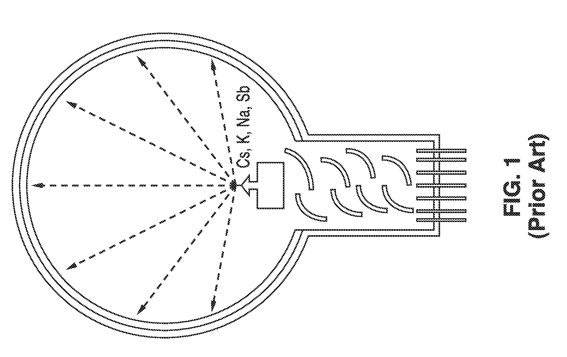
Existing technologies for fabricating large-area photosensors, which have not been significantly improved since the 1960s, are outdated, expensive, low-quality, and labor intensive. FIG. 1 depicts a typical large-area photomultiplier tube (LAPMT) based on vacuum tube technology and dynode electron multipliers that are essentially hand-made, expensive and very problematic to produce in sufficiently large quantities.
The structures of these existing devices suffer from numerous drawbacks, many of which arise from their “ship-in-a-bottle” type of design, in which all the elements of the device are retained, interconnected, and supported within a single enveloping glass-tube housing.
The LAPMT shown in FIG. 1 has a configuration whose manufacture is intrinsically labor-intensive, with the glass bulb and dynode column each accounting for about one half of the manufactured cost of an LAPMT.
The complexity and cost of the bulb portion is significantly influenced by the necessity of having a long dynode column leading into the spherical bulb portion.
HPDs are very expensive to produce for a number of reasons.
First, there is the high cost of the Avalanche Photo Diodes themselves, which cannot merely comprise a multi-cell Geiger-mode APD, because of their large dead area (approximately 50%) for direct photoelectron detection.
Second, there is a need for high voltage supplies to an ordinary APD.
The direct use of ordinary APDs is thus fraught with numerous drawbacks, while they are also very sensitive to even slight amounts of light overexposure, and in other ways are too fragile for a number of applications.
Still further, an APD provides only a very low gain (thousands), with an output signal that requires careful shielding and significant amplification using expensive preamplifiers.
Furthermore, existing LAPMT device solutions are subject to a number of serious performance problems, including but not limited to the following: (1) very low photoelectron collection efficiency, such as only approximately 70%, which is often unlisted on manufacturer data sheets; (2) modest quantum efficiency; (3) non-uniform quantum efficiency; (4) high sensitivity to geomagnetic fields; (5) complicated and expensive mounting options; (6) highly fragile packaging which was dramatically demonstrated in the Super Kamiokande disaster; and (7) lack of single-photon resolution.
The available devices, such as silicon detectors, for instance like the avalanche photo diodes (APDs) utilized for the readout of crystals in the Compact Muon Solenoid (CMS) experiment at the Large Hadron Collider (LHC) at CERN in Geneva, are considered too small and costly for use in experiments requiring a very large sensitive area.

Method used


Image

  • Vacuum photosensor device with electron lensing
  • Vacuum photosensor device with electron lensing
  • Vacuum photosensor device with electron lensing

Examples


embodiment 10

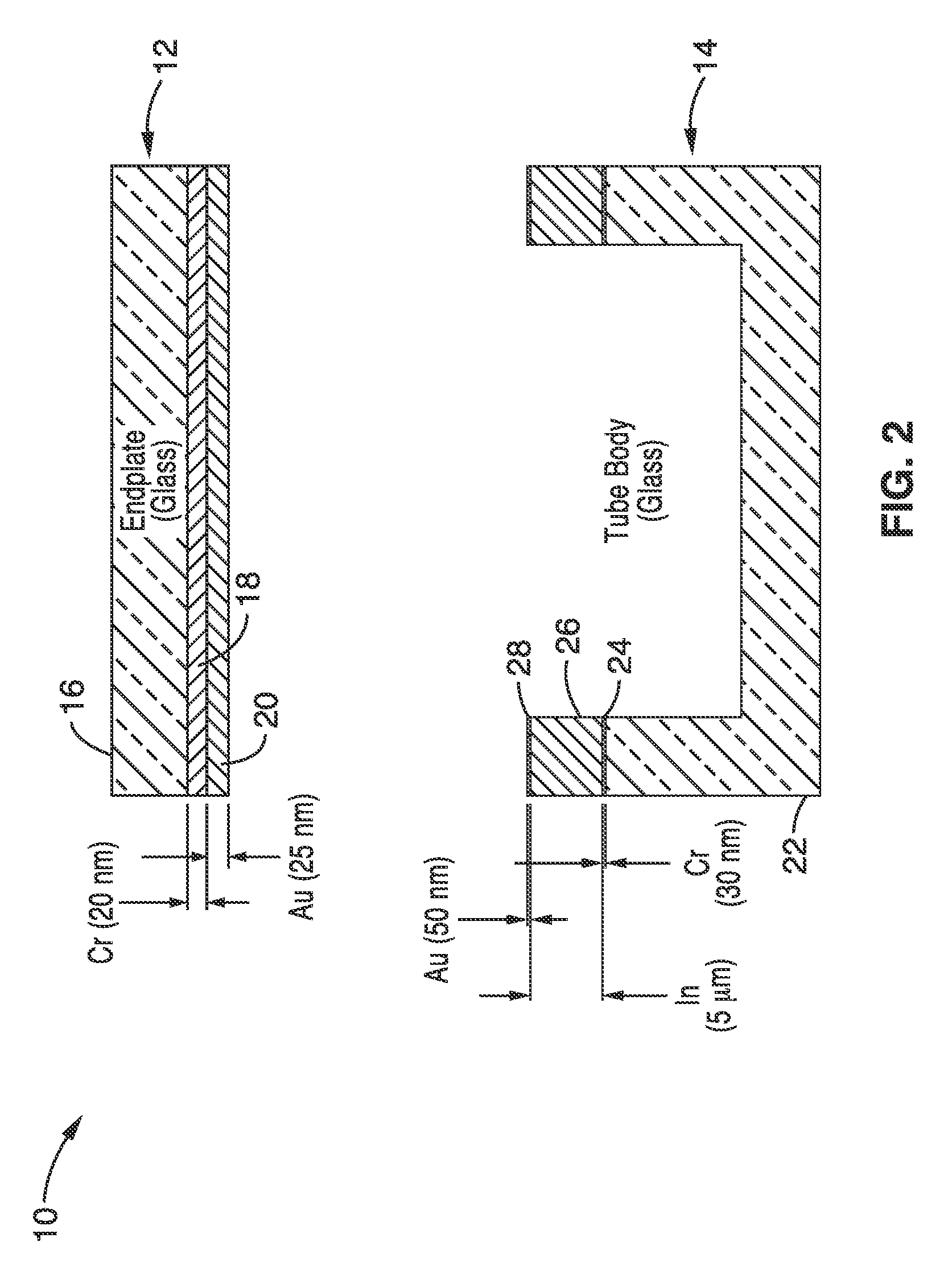
[0064]Referring first to FIG. 2, an embodiment 10 of an oxide-free sealing means for an ABALONE photosensor device according to the present invention is shown. In FIG. 2, a glass endplate 12 is shown configured for being hermetically sealed to a tube body 14. Layers of material are deposited on both portions to be joined, specifically, the endplate glass 12 of a material 16 and tube body 14 of a material 22 In preparation for sealing. A layer of Chromium (Cr) 18, for example about 20 nm thick, is overlaid with Gold (Au) 20, for example of 25 nm thick, on one element with the other elements being overlaid with a layer of Chromium (Cr) 24 of about 30 nm, Indium (In) 26 of about 5 um and Gold (Au) 28 of about 50 nm. In response to heat the Indium reacts with the Gold to form a Gold-Indium interface.

[0065]The primary role of the Chromium film in the sealing means is to establish a chemical contact with glass or quartz. Chromium breaks the chemical bond between Silicon and Oxygen in thes...

embodiment 50

[0067]FIG. 3 illustrates an uninterrupted vacuum production line embodiment 50, exemplified as the UHV (ultra high vacuum) transfer facility which the inventors have developed at the University of California at Davis. This device is utilized for photocathode deposition and sealing the concave transparent housing to the base plate while retaining an ultrahigh vacuum. The production line 50 is shown with four ultrahigh vacuum chambers 52, 54, 56 and 58, with base pressure lower than 5×10⁻¹⁰ Torr, for fabricating the devices. Each chamber, for example, can be pumped with turbomolecular and ion pumps, with the vacuum quality controlled by quadrapole mass spectrometers. Prototype components travel from one chamber to another for appropriate processing, and finally meet in the central chamber 54 for hermetic sealing.

[0068]A preferred factory will have three separate and specialized lines of chambers, one for each glass component. Those lines would meet in a pair of sealing chambers. The s...

embodiment 90

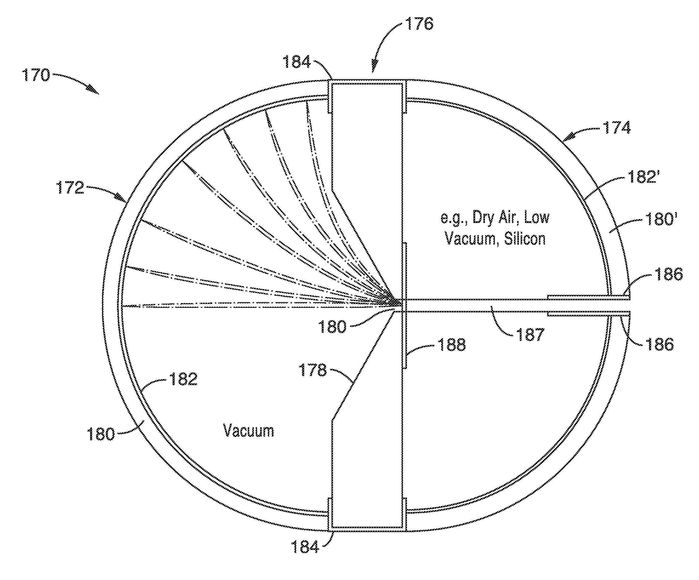
[0084]Referring now to FIG. 5 through FIG. 9, an embodiment 90 of an open architecture vacuum photosensor device according to the present invention is illustrated. The vacuum seal is facilitated by the oxide-free Indium sealing means previously described, which can be performed simply and rapidly. In addition, the resultant two thin-film seals act together as the only necessary high voltage throughputs to the device. It will be appreciated that no electrode feedthroughs are necessary, which simplifies the production process and utility of the inventive ABALONE photosensor devices.

[0085]The embodiment shown in FIG. 5 through FIG. 9 comprises a vacuum housing portion, herein concave shaped as a first housing (hemisphere) 92 of optically transparent dielectric material 94 having a conductive layer 96 as a photocathode and shown hermetically sealed to a base plate 102 having a through hole 104 into which a readout 106 is sealed. FIG. 5 depicts the hemisphere, base plate and readout in a...


PUM


Abstract

A scalable vacuum photosensor configured to simplify mass production with a housing having an evacuated first side at an ultrahigh vacuum and a second side which does not require high vacuum. The first side of the device is sealed to a base plate, having a central electron readout element, using an oxide-free sealing technique, with the deposited sealing areas serving as high voltage throughputs from the first to second sides. A conductive photocathode layer on the transparent first side converts photons to photoelectrons and concentrates the photoelectrons upon the readout. The first and second sides together form an electrostatic lens for accelerating and focusing photoelectrons upon the readout, preferably having a scintillator which generates secondary light measured by an optical detector in the second side of the housing.

Description

CROSS-REFERENCE TO RELATED APPLICATIONS[0001]This application is a 35 U.S.C. §111(a) continuation of PCT international application number PCT / US2011 / 036554 filed on May 13, 2011, incorporated herein by reference in its entirety, which is a nonprovisional of U.S. provisional patent application Ser. No. 61 / 334,919 filed on May 14, 2010, incorporated herein by reference in its entirety. Priority is claimed to each of the foregoing applications.[0002]The above-referenced PCT international application was published as PCT International Publication No. WO 2011 / 143638 on Nov. 17, 2011 and republished on Mar. 1, 2012.STATEMENT REGARDING FEDERALLY SPONSORED RESEARCH OR DEVELOPMENT[0003]This invention was made with Government support under Grant DE-FC52-04NA25684 awarded by DOE. The Government has certain rights in the invention.INCORPORATION-BY-REFERENCE OF MATERIAL SUBMITTED ON A COMPACT DISC[0004]Not ApplicableNOTICE OF MATERIAL SUBJECT TO COPYRIGHT PROTECTION[0005]A portion of the materia...

Claims


Application Information

Patent Timeline
Patent Type & Authority Patents(United States)
IPC IPC(8): H01J40/14H01J43/06H01J43/00H01J40/16
CPCH01J43/06H01J43/00H01J40/16
Inventor FERENC, DANIEL
Owner RGT UNIV OF CALIFORNIA
Learn More