Opto-electric combined circuit board and electronic devices

a combined circuit board and opto-electric technology, applied in the direction of optical elements, circuit optical details, instruments, etc., can solve the problems of braking and cracking, high disadvantage, liable to be broken, etc., and achieve good flexural durability and good communication function.

Inactive Publication Date: 2015-06-30
RESONAC CORPORATION
View PDF9 Cites 35 Cited by
  • Summary
  • Abstract
  • Description
  • Claims
  • Application Information

AI Technical Summary

Benefits of technology

[0013]The opto-electric combined circuit board of the present invention and the electronic devices prepared by using the above opto-electric combined circuit board have such a very good flexural durability that breaking and cracking are not generated even after repeating bending over a long period of time and can maintain a good communication function.

Problems solved by technology

However, the present inventors have found that a structure in which an optical waveguide film is partially separated from a flexible electric wiring board involves the problem that when bending is actually carried out by a hinge, particularly when the electronic device has a slide structure and further has a structure in which a bending part moves following sliding in the state that an opto-electric combined circuit board is bent at the bending part as a center, an optical waveguide is liable to deviate to a lateral direction against the flexible electric wiring board and an adhesion surface thereof and that the above lateral deviation allows the optical waveguide to move while deforming when it slides, so that it is liable to be broken.
A side guide mechanism can be provided in order to prevent the above deviation of the optical waveguide to the lateral direction, but it is very troublesome and highly disadvantageous in electronic devices which are required to be reduced in a size.
That is, in an opto-electric combined circuit board having a separated structure shown in the patent document 2, the problem that ultimately, a stress is exerted on an optical waveguide part to result in causing braking and cracking has not yet come to be solved.

Method used


Image

  • Opto-electric combined circuit board and electronic devices
  • Opto-electric combined circuit board and electronic devices
  • Opto-electric combined circuit board and electronic devices

Examples


example 1

(1-1) Preparation of an Optical Waveguide

Preparation of a Resin Film for Forming a Cladding Layer:

[0079]Weighed into a wide mouth plastic bottle were 48 parts by mass of a phenoxy resin (trade name: Phenotohto YP-70, manufactured by Tohto Kasei Co., Ltd.) as the binder polymer (A), 49.6 parts by mass of alicyclic diepoxycarboxylate (trade name: KRM-2110, molecular weight: 252, manufactured by Asahi Denka Co., Ltd.) as the photopolymerizable compound (B), 2 parts by mass of a triphenylsulfonium hexafluoroantimonate salt (trade name: SP-170, manufactured by Asahi Denka Co., Ltd.) as the photopolymerization initiator (C), 0.4 part by mass of SP-100 (trade name, manufactured by Asahi Denka Co., Ltd.) as a sensitizer and 40 parts by mass of propylene glycol monomethyl ether acetate as an organic solvent, and the mixture was stirred for 6 hours on the conditions of a temperature of 25° C. and a revolution of 400 rpm by means of a mechanical stirrer, a shaft and a propeller to prepare a re...

reference example 1

[0099]The optical waveguide simple body prepared in Example 1 was used to carry out a bending durability test as was the case with the opto-electric combined circuit board prepared in Example 1. The results thereof are shown in Table 1.

[0100]

TABLE 1Bendingbending durabilityradius (R) (mm)test (frequency)Example 11.5350,0001.0100,000Comparative1.510,000Example 11.01,000Comparative1.520,000Example 21.05,000Reference1.550,000Example 11.010,000

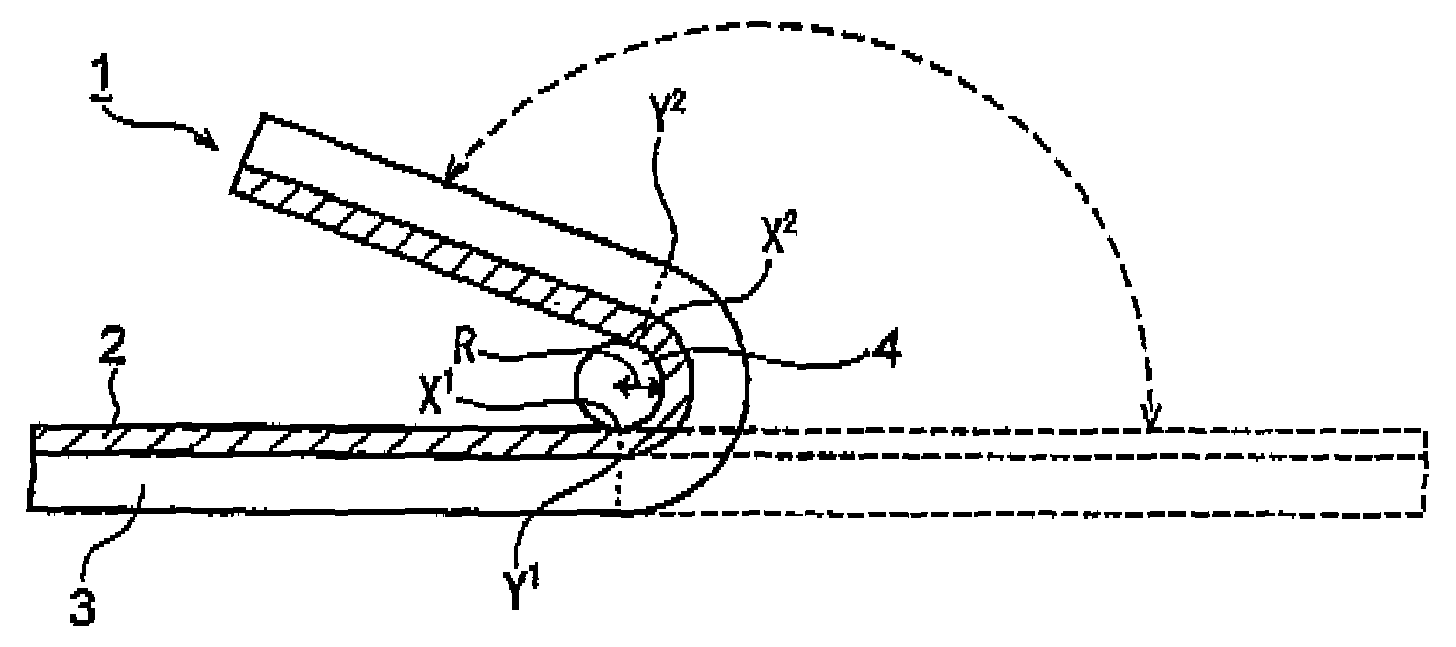
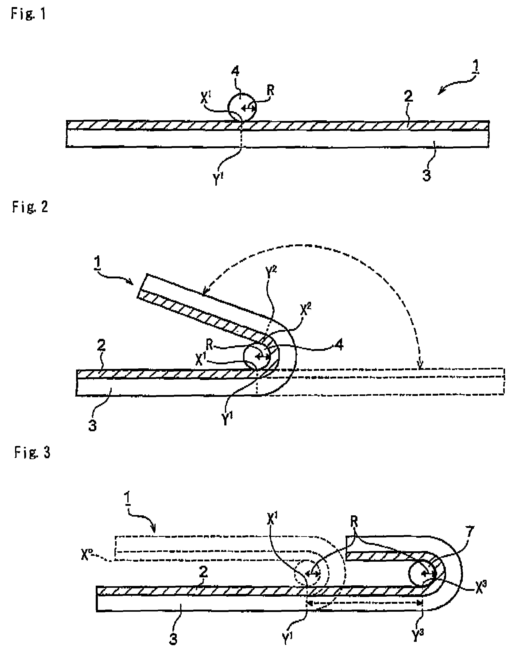
[0101]As shown in Table 1, it can be found that a bending durability of the opto-electric combined circuit board is dramatically enhanced by controlling the core part of the optical waveguide and the electric wiring in the bending part so that they are not overlapped in a projection plane.


PUM


Abstract

The present invention relates to a flexible opto-electric combined circuit board in which an optical waveguide film provided with a core and a clad is bonded to a flexible electric wiring board, wherein a reinforcing material is provided to at least a part of an optical waveguide film side in a bent part and electronic devices prepared by using the above flexible opto-electric combined circuit board.Capable of being provided are an opto-electric combined circuit board in which an optical waveguide film is bonded to a flexible electric wiring board and in which braking and cracking are not generated by bending or folding back and electronic devices prepared by using the above opto-electric combined circuit board.

Description

BACKGROUND OF THE INVENTION[0001]The present invention relates to an opto-electric combined circuit board in which optical wirings having a flexibility are combined with electrical wirings and an electronic device prepared by using the above board.RELATED ART[0002]In recent years, in high speed & high density signal transmission between electronic devices and between wiring boards, transmission through conventional electric wirings is restricted in a rise in a speed and a density due to barriers brought about by mutual interference and attenuation of signals. In order to break through the above barriers, a technique for connecting electronic devices and wiring boards with each other by means of light, so-called optical interconnection is investigated. A polymer optical waveguide attracts attentions as an optical transmission line in terms of easier processing, a lower cost, a higher freedom of wirings and a possible rise in a density.[0003]In particular, it is investigated to use an...

Claims


Application Information

Patent Timeline
Patent Type & Authority Patents(United States)
IPC IPC(8): G02B6/00H05K1/02G02B6/122G02B6/43H05K1/03
CPCG02B6/1221H05K1/0274G02B6/43H05K1/028H05K1/0393G02B6/424G02B6/4274G02B6/4293G02B6/122
Inventor KURODA, TOSHIHIROSHIBATA, TOMOAKIYAGI, SHIGEYUKI
Owner RESONAC CORPORATION
Why Eureka
Try Eureka