Optical waveguide device, optical interferometer, and method for producing optical waveguide device

a control method and waveguide technology, applied in optics, instruments, electrical devices, etc., can solve the problems of difficult to grasp the situation of light transmitting inside the channel with accuracy, and difficult to grasp the intensity of light inputted to the optical coupler with accuracy, etc., to achieve simple and easy configuration

Active Publication Date: 2015-06-30
NEC CORP
View PDF16 Cites 8 Cited by
  • Summary
  • Abstract
  • Description
  • Claims
  • Application Information

AI Technical Summary

Benefits of technology

[0037]According to some aspects of the present invention, it becomes possible to independently perform control of a phase difference and losses which are given to any two ones of lights each transmitting through a corresponding one of a plurality of optical waveguide devices, in a simple and easy configuration.

Problems solved by technology

Meanwhile, merely increasing the bit rate of a signal in order to enhance the frequency efficiency leads to a problem of cross talk between the channels.
For this reason, with respect to the LN modulator 300 shown in FIG. 12, there has been also a problem that it is difficult to grasp the situation of light transmitting inside thereof with accuracy.
For this reason, in the configuration disclosed in PTL3, there is a problem that it is difficult to grasp the intensity of light inputted to the optical coupler with accuracy.

Method used


Image

  • Optical waveguide device, optical interferometer, and method for producing optical waveguide device
  • Optical waveguide device, optical interferometer, and method for producing optical waveguide device
  • Optical waveguide device, optical interferometer, and method for producing optical waveguide device

Examples


first exemplary embodiment

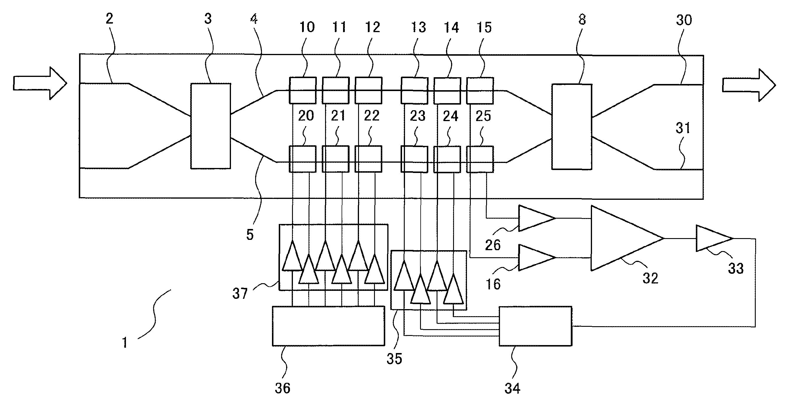
[0051]In this first exemplary embodiment, there is proposed a configuration of an optical waveguide device which, between the first optical waveguide and the second optical waveguide included in the Mach-Zehnder type optical modulator composed of a semiconductor material, gives a desired phase difference to the lights, and simultaneously, causes light densities of the lights to be equally balanced.

[0052]In this first exemplary embodiment, the light intensities of lights each transmitting through the waveguides are monitored at positions anterior to the optical coupler in a modulated light traveling direction, and voltages applied to an electrode of the first optical waveguide and an electrode of the second optical waveguide are controlled on the basis of the monitored light intensities. A specific example of a configuration therefor is shown in FIG. 1.

[0053]FIG. 1 is a diagram illustrating a configuration of an optical waveguide device of the first exemplary embodiment of the presen...

second exemplary embodiment

[0099]Next, a second exemplary embodiment of the present invention will be described. An optical waveguide device of the second exemplary embodiment is an optical waveguide device resulting from changing the shapes of the control electrodes provided on the optical waveguides 4 and 5 in the optical waveguide device, shown in FIG. 1, according to the first exemplary embodiment.

[0100]In FIG. 8 and FIG. 9, there are illustrated the shapes of the electrodes of the optical waveguide device of the second exemplary embodiment. In FIGS. 8 and 9, there are illustrated only electrodes 41 to 46 as substitutes for the electrodes 13 and 14 and the electrodes 23 and 24 which are provided on the first and second optical waveguides 4 and 5 in FIG. 1. The configuration of the optical waveguide device of the second exemplary embodiment is the same as that of the optical waveguide device of the first exemplary embodiment, except that the electrodes 41 to 46 are provided as substitutes for the electrode...

third exemplary embodiment

[0108]Next, as a third exemplary embodiment to which this device is applied, a configuration that a loss difference between a plurality of optical waveguides is kept constant and amounts of phase variations given to the transmitting lights are controlled will be described.

[0109]FIG. 10 is a diagram illustrating a configuration of an optical waveguide device of the third exemplary embodiment. The optical waveguide device shown in FIG. 10 is an inphase / quadrature (I / Q) modulator 50 in which two Mach-Zehnder type optical modulators are connected in parallel to each other. The I / Q modulator modulates an I component (a real axis) and a Q component (an imaginary axis) of a light signal independently, superimposes information onto the amplitude and the phase on a complex plane, and performs multi-value modulation.

[0110]As shown in FIG. 10, the I / Q modulator 50 includes an optical divider 51, an I modulator 52, a Q modulator 53 and an optical coupler 55. The I modulator 52 and the Q modulat...


PUM

PropertyMeasurementUnit
refractive indexaaaaaaaaaa
phaseaaaaaaaaaa

Abstract

In order to independently perform control of a phase difference and a loss of light transmitting through an optical waveguide in a simple and easy configuration, an optical waveguide device includes an optical waveguide provided with two electrodes each supplied with a corresponding one of two signals; and a control unit for controlling the two signals so as to cause a phase variation and a loss variation which are caused in light transmitting through the optical waveguide by the two signals to each have a predetermined value.

Description

[0001]This application is a National Stage Entry of PCT / JP2012 / 064608 filed on May 31, 2012, which claims priority from Japanese Patent Application 2011-123204 filed on Jun. 1, 2011, the contents of all of which are incorporated herein by reference, in their entirety.TECHNICAL FIELD[0002]The present invention relates to an optical waveguide device, an optical interferometer and a control method for an optical waveguide device.BACKGROUND ART[0003]In optical communication systems, large-capacity transmission based on high-speed transmission and wavelength multiplexing has been promoted. Particularly, in optical communication systems for trunk line, wavelength multiplexing communication has been widely used. In the wavelength multiplexing communication, a wavelength channel interval is prescribed and when the wavelength channel interval within a band of an optical fiber amplifier is 50 GHz, it is possible to use approximately one hundred channels.[0004]Here, when representing a channel...

Claims


Application Information

Patent Timeline
Patent Type & Authority Patents(United States)
IPC IPC(8): G02F1/035G02F1/01G02F1/225
CPCG02F1/011G02F1/0123G02F1/225H04B10/5057
Inventor SATO, KENJISATOH, MINETO
Owner NEC CORP
Why Eureka
Try Eureka