Semiconductor device having an oxide semiconductor with a crystalline region and manufacturing method thereof

a semiconductor and oxide technology, applied in the direction of semiconductor devices, electrical appliances, transistors, etc., can solve the problem of low on/off ratio of transistors, and achieve the effect of simple method, reduced size or number, and increased operation speed of the circuit included in the semiconductor devi

Active Publication Date: 2015-07-28
SEMICON ENERGY LAB CO LTD
View PDF244 Cites 31 Cited by
  • Summary
  • Abstract
  • Description
  • Claims
  • Application Information

AI Technical Summary

Benefits of technology

[0014]The present invention is made in view of the foregoing technical background. Therefore, an object of the present invention is to provide a semiconductor device in which transistors with different characteristics, specifically, a transistor with excellent dynamic characteristics (on characteristics or frequency characteristics (referred to as f characteristics)) and a transistor having a reduced off-state current, are provided over one substrate. Further, another object is to provide a simple method for manufacturing the semiconductor device.
[0026]According to one embodiment of the present invention, a crystalline region included in an oxide semiconductor layer is used as a channel formation region, whereby operation speed of the circuit included in a semiconductor device can be increased. In addition, a circuit is formed using a transistor in which a purified oxide semiconductor is used, whereby operation of the circuit included in a semiconductor device can be stabilized. Further, off-state current reduced to 1×10⁻¹³ A or lower, whereby a storage capacitor included in a semiconductor device can be reduced in size or in number. Further, a semiconductor device including transistors with different characteristics over one substrate can be provided. Furthermore, the semiconductor device can be manufactured by a simple method.

Problems solved by technology

Such a low on / off ratio of the transistor is due to large off-state current.

Method used


Image

  • Semiconductor device having an oxide semiconductor with a crystalline region and manufacturing method thereof
  • Semiconductor device having an oxide semiconductor with a crystalline region and manufacturing method thereof
  • Semiconductor device having an oxide semiconductor with a crystalline region and manufacturing method thereof

Examples


embodiment 1

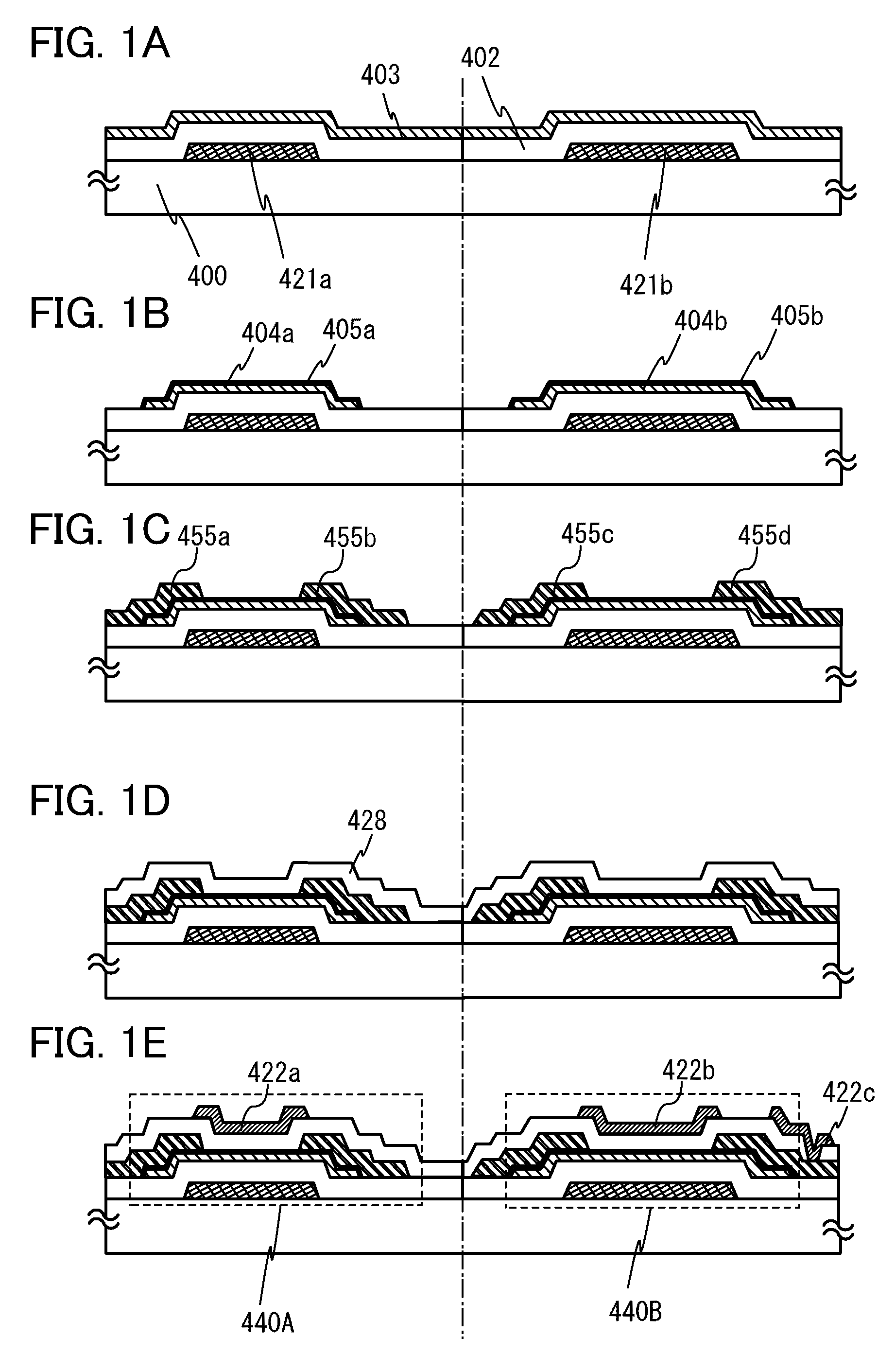
[0056]In this embodiment, one embodiment of a substrate provided with a circuit of a display device and a manufacturing method of the substrate provided with a circuit as one embodiment of a semiconductor device and a manufacturing method of the semiconductor device will be described with reference to FIGS. 1A to 1E.

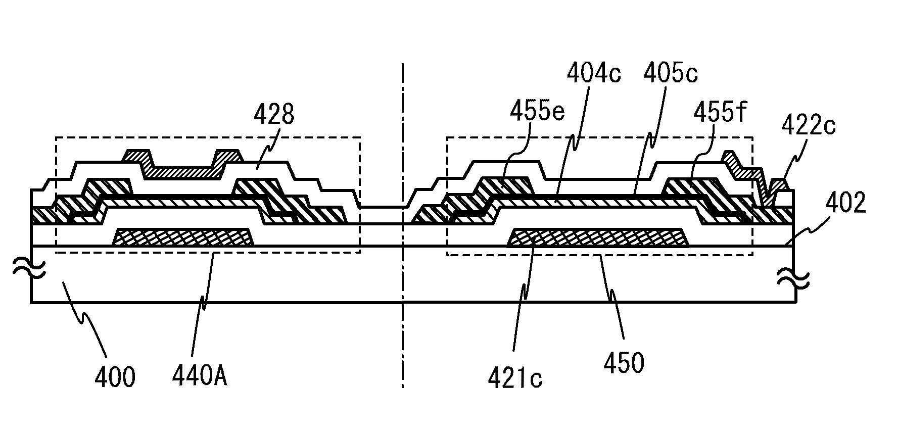
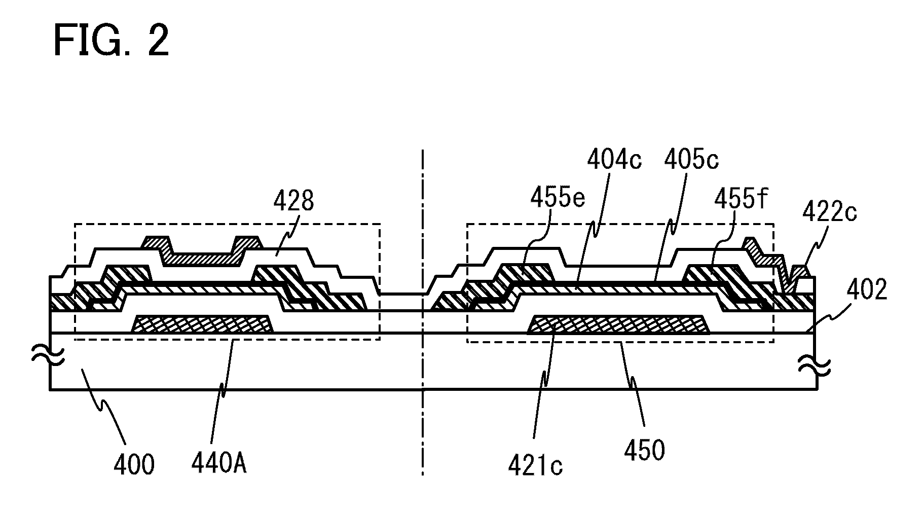
[0057]FIG. 1E illustrates an example of a cross-sectional structure of a plurality of transistors formed over a substrate provided with a circuit of a display device. Transistors 440A and 440B illustrated in FIG. 1E each have a kind of four-terminal structure in which a pair of electrode layers which are provided on opposite sides from each other with respect to a channel formation region of an oxide semiconductor layer, each with an insulating film arranged therebetween. Note that a so-called dual-gate transistor in which a pair of electrode layers which are provided on opposite sides from each other with respect to a channel formation region of an oxide semiconductor l...

embodiment 2

[0182]In Embodiment 2, an example of forming an inverter circuit of a driver circuit using two transistors each having a four-terminal structure in which a pair of electrode layers which are provided on opposite sides from each other with respect to a channel formation region of an oxide semiconductor layer, each with an insulating film arranged therebetween is described with reference to FIGS. 3A, 3B, and 3C. Transistors in FIG. 3A are the same as the transistors 440A and 440B in FIG. 1E of Embodiment 1, and thus the same parts are denoted by the same reference numerals.

[0183]A driver circuit for driving a pixel portion may be provided in the periphery of the pixel portion, and is formed using an inverter circuit, a capacitor, a resistor, or the like. In one embodiment of the inverter circuit, the inverter circuit is formed using two n-channel transistors in combination. For example, there are an inverter circuit having a combination of an enhancement transistor and a depletion tra...

embodiment 3

[0194]In this embodiment, an example of manufacturing a pulse output circuit using a transistor in which a pair of electrode layers which are provided on opposite sides from each other with respect to a channel formation region of an oxide semiconductor layer, each with an insulating film arranged therebetween. Further, an example of manufacturing a shift register by connecting a plurality of such pulse output circuits will be described with reference to FIGS. 4A to 4C and FIGS. 5A and 5B.

[0195]Note that a transistor is an element having at least three terminals of a gate, a drain, and a source. The transistor has a channel region between a drain region and a source region, and current can flow through the drain region, the channel region, and the source region. Here, since the source and the drain of the transistor may change depending on the structure, the operating condition, and the like of the transistor, it is difficult to define which is a source or a drain. Therefore, region...


PUM


Abstract

An oxide semiconductor layer which is intrinsic or substantially intrinsic and includes a crystalline region in a surface portion of the oxide semiconductor layer is used for the transistors. An intrinsic or substantially intrinsic semiconductor from which an impurity which is to be an electron donor (donor) is removed from an oxide semiconductor and which has a larger energy gap than a silicon semiconductor is used. Electrical characteristics of the transistors can be controlled by controlling the potential of a pair of conductive films which are provided on opposite sides from each other with respect to the oxide semiconductor layer, each with an insulating film arranged therebetween, so that the position of a channel formed in the oxide semiconductor layer is determined.

Description

TECHNICAL FIELD[0001]The present invention relates to a semiconductor device including a transistor.[0002]Note that the semiconductor device in this specification refers to any device that can function by utilizing semiconductor characteristics, and semiconductor elements and circuits, electro-optic devices including semiconductor elements and circuits, and electronic devices including semiconductor elements and circuits are all semiconductor devices.BACKGROUND ART[0003]In recent years, a technique by which transistors are formed using semiconductor thin films formed over a substrate having an insulating surface has been attracting attention. A transistor is used for a semiconductor device typified by a liquid crystal television. As a semiconductor thin film that can be applied to the transistors, a silicon-based semiconductor material is known, and an oxide semiconductor attracts attention as another material.[0004]A transistor is manufactured mainly using a semiconductor material ...

Claims


Application Information

Patent Timeline
Patent Type & Authority Patents(United States)
IPC IPC(8): H01L29/12H01L27/12H01L29/786H01L21/02
CPCH01L27/1251H01L27/1225H01L21/02603H01L29/7869H01L29/78693H01L29/78696H01L29/24H01L27/0883H01L29/045H01L29/4908H01L2924/13069H01L29/04H01L29/78669H01L29/78678H01L27/127H01L27/1288
Inventor YAMAZAKI, SHUNPEIKOYAMA, JUNMIYAKE, HIROYUKI
Owner SEMICON ENERGY LAB CO LTD
Why Eureka
Try Eureka