3-D nonvolatile memory devices and methods of manufacturing the same

a nonvolatile memory and non-volatile technology, applied in the field of semiconductor devices, can solve the problems of lowering the erase speed, slow erase speed, and slow erase speed

Active Publication Date: 2015-08-25
SK HYNIX INC
View PDF7 Cites 7 Cited by
  • Summary
  • Abstract
  • Description
  • Claims
  • Application Information

AI Technical Summary

Benefits of technology

[0012]An embodiment of this disclosure provides a 3-D nonvolatile memory device and a method of manufacturing the same which can secure an erase characteristic by generating a sufficient number of holes when an erase operation is performed.

Problems solved by technology

The known 3-D nonvolatile memory device is problematic in that the erase speed is slow because the number of holes generated by the GIDL current is insufficient and the erase speed is lowered because sufficient holes are not supplied to some of the memory cells.
In particular, in the known 3-D nonvolatile memory device, since the strings are vertically arranged from the substrate 10, the supply of holes becomes more difficult as the length of the channel layer CH increases.
As a result, the speed of an erase operation is further reduced, and thus the memory device has poor performance.

Method used


Image

  • 3-D nonvolatile memory devices and methods of manufacturing the same
  • 3-D nonvolatile memory devices and methods of manufacturing the same
  • 3-D nonvolatile memory devices and methods of manufacturing the same

Examples


first embodiment

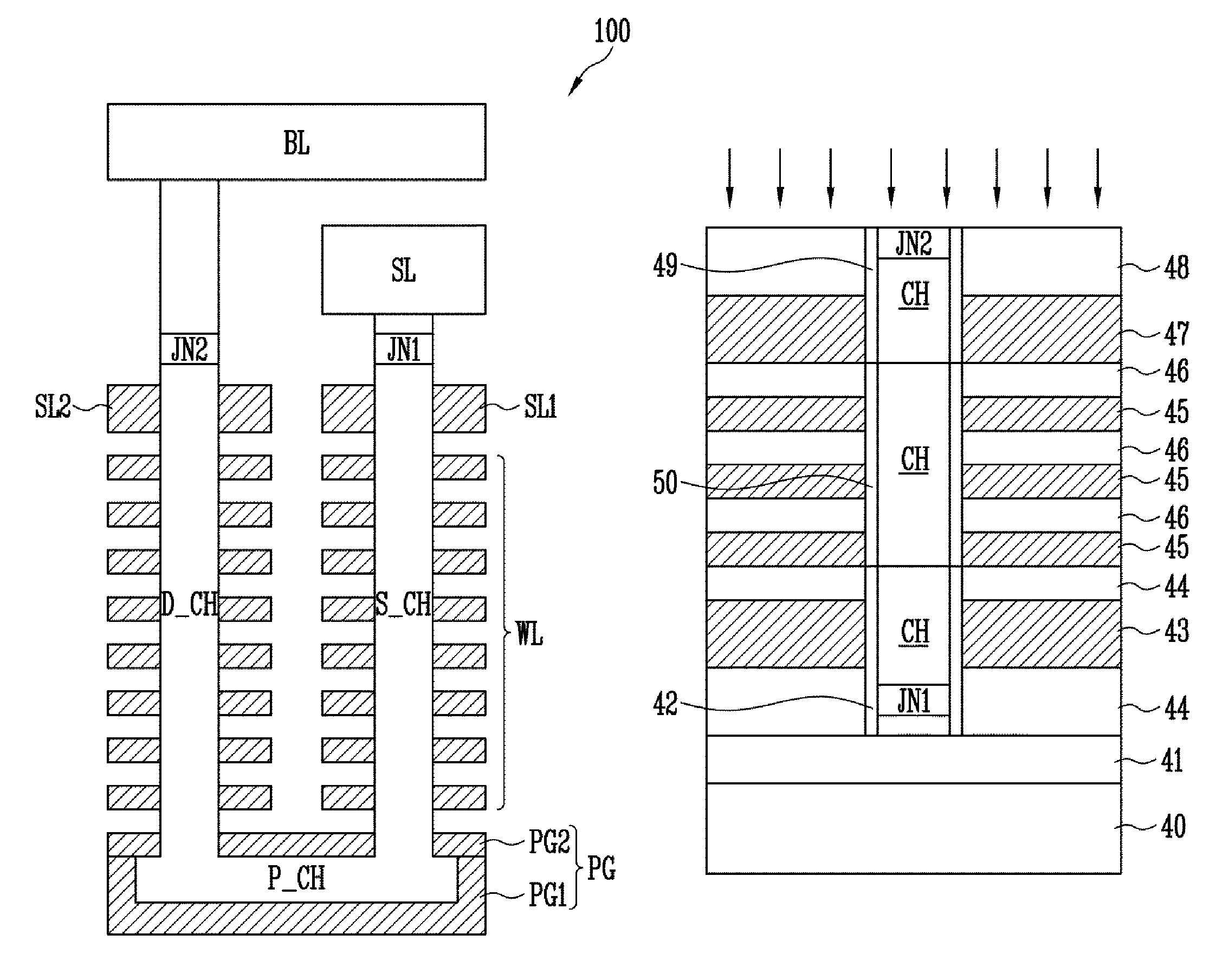
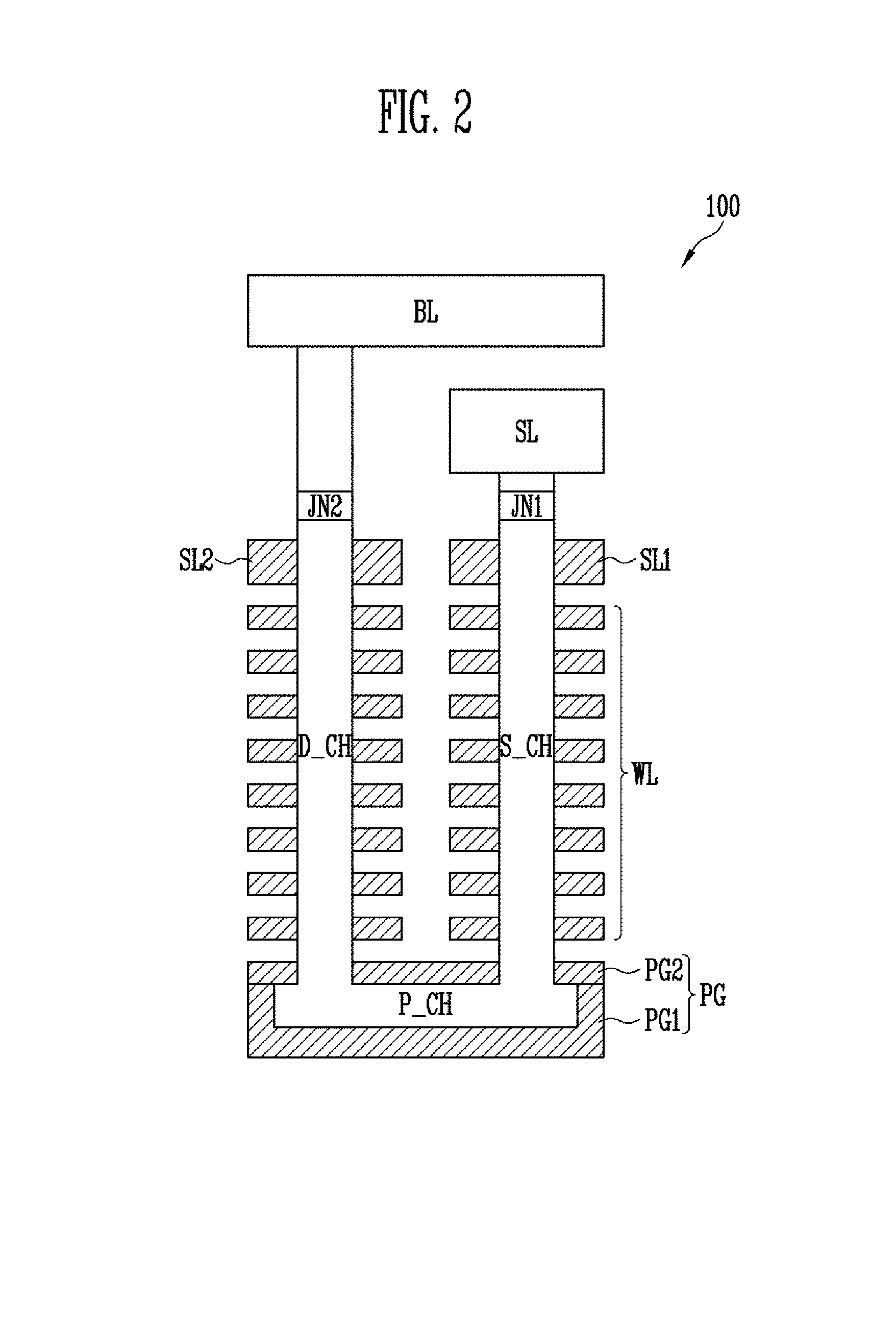
[0031]FIG. 2 is a cross-sectional view showing the structure of a 3-D nonvolatile memory device according to this disclosure. In this figure, only a plurality of word lines, first and second select lines, a bit line, and a source line are chiefly illustrated, and an interlayer insulating layer interposed between the lines is not shown, for convenience of description.

[0032]As shown in FIG. 2, the 3-D nonvolatile memory device 100 according to the first embodiment of this disclosure may include a channel layer (P_CH, S_CH, and D_CH) protruded from a substrate and a plurality of memory cells stacked along the channel layer (P_CH, S_CH, and D_CH). Each of strings may be formed substantially in a U form.

[0033]The channel layer (P_CH, S_CH, and D_CH) may include a pipe channel layer P_CH buried in a pipe gate PG and a pair of a source-side channel layer S_CH and a drain-side channel layer D_CH coupled to the pipe channel layer P_CH and protruded from the pipe gate PG. The pipe gate PG may...

second embodiment

[0047]FIG. 6 is a cross-sectional view showing the structure of a 3-D nonvolatile memory device according to this disclosure. In this figure, only a plurality of word lines, first and second select lines, a bit line, and a source line are chiefly illustrated, and an interlayer insulating layer interposed between the lines is not shown, for convenience of description.

[0048]As shown in FIG. 6, in the 3-D nonvolatile memory device 200 according to the second embodiment of this disclosure, each of strings may be formed substantially in a U form, and a plurality of memory cells coupled in series between two first select transistors and two second select gates forms each of the strings. The remaining elements of the 3-D nonvolatile memory device 200 according to the second embodiment are the same as those of the 3-D nonvolatile memory device 100 according to the first embodiment.

[0049]If two first select lines SL1-1 and SL1-2 and two second select lines SL2-1 and SL2-2 may be formed as in...

third embodiment

[0054]FIG. 7 is a cross-sectional view showing the structure of a 3-D nonvolatile memory device according to this disclosure. In this figure, only a plurality of word lines, first and second select lines, a bit line, and a source line are chiefly illustrated, and an interlayer insulating layer interposed between the lines is not shown, for convenience of description.

[0055]As shown in FIG. 7, the 3-D nonvolatile memory device 300 according to the third embodiment of this disclosure may include strings each formed in a U form and a third junction JN3 interposed between the end of one side of channel layer (P_CH, S_CH, and D_CH), forming the U form, and a first junction JN1 and configured to have an N type impurity doped therein. The remaining elements of the third embodiment have the same construction as those of the 3-D nonvolatile memory device 200 according to the second embodiment.

[0056]The 3-D nonvolatile memory device according to the third embodiment may be driven on the same c...


PUM


Abstract

A three-dimensional (3-D) nonvolatile memory device includes a channel layer protruded from a substrate, a plurality of memory cells stacked along the channel layer, a source line coupled to the end of one side of the channel layer, a bit line coupled to the end of the other side of the channel layer, a first junction interposed between the end of one side of the channel layer and the source line and configured to have a P type impurity doped therein, and a second junction interposed between the end of the other side of the channel layer and the bit line and configured to have an N type impurity doped therein.

Description

CROSS-REFERENCE TO RELATED APPLICATION[0001]Priority to Korean patent application number 10-2011-0109947 filed on Oct. 26, 2011, the entire disclosure of which is incorporated by reference herein, is claimed.BACKGROUND[0002]1. Technical Field[0003]Embodiments of this disclosure relate to semiconductor devices and methods of manufacturing the same and, more particularly, to nonvolatile memory devices having three-dimensional (3-D) structures and methods of manufacturing the same.[0004]2. Related Art[0005]A nonvolatile memory device retains data stored therein although the supply of power is cut off. As the recent improvement of the degree of integration of 2-D memory devices in which memory cells may be formed in a single layer over a silicon substrate reaches the limit, there is proposed a 3-D nonvolatile memory device in which memory cells are vertically stacked in multiple layers from a silicon substrate.[0006]The structure of a known 3-D nonvolatile memory device and problems the...

Claims


Application Information

Patent Timeline
Patent Type & Authority Patents(United States)
IPC IPC(8): G11C5/02G11C16/04G11C16/14H01L21/822H01L27/115
CPCG11C16/14H01L21/8221H01L27/1157H01L27/11524H01L27/11578H01L27/11582H01L27/11556G11C16/0408H10B41/27H10B43/27H01L27/0688H10B41/35H10B43/20H10B43/35
Inventor OH, SANG HYUNARITOME, SEIICHILEE, SANG BUM
Owner SK HYNIX INC
Why Eureka
Try Eureka