Transistor and method for manufacturing the same

a technology of transistors and transistors, applied in the field of semiconductor devices, can solve the problems of data loss in capacitors, increased threshold voltage or leakage current at junction regions, and devices with a tendency to have a reduced design rule, so as to prevent an increase in the ion concentration of storage nodes

Inactive Publication Date: 2005-12-01
SK HYNIX INC
View PDF4 Cites 4 Cited by
  • Summary
  • Abstract
  • Description
  • Claims
  • Application Information

AI Technical Summary

Benefits of technology

[0015] The present invention has been made in view of the above-mentioned problems, and it is an object of the invention to provide a transistor of a DRAM cell having asymmetrical ion concentration profiles of bit line and storage nodes while preventing an ion diffusion between the bit line and storage nodes to prevent an increase in the ion concentration of the storage node, thereby being capable of securing desired refresh characteristics of the DRAM cell.

Problems solved by technology

However, recently-developed memory devices have a tendency to have a reduced design rule, so that they have a reduced channel length between a source and a drain in each transistor.
As a result, an increase in threshold voltage or an increase in the amount of leakage current at junction regions may occur.
For this reason, the data stored in the capacitors may be lost.
In this case, however, an abrupt increase in the ion concentration of channel regions occurs, thereby causing a degradation in refresh characteristics.
Thus, when an additional ion implantation process is performed only for the junctions to contact the bit lines, that is, the bit line nodes, in accordance with the conventional method, the impurity concentration of the channel regions is abnormally increased due to the reduced design rule of the DRAM device to be manufactured through the conventional method.
As a result, the doping profile established between the channel and the junction is rendered to be sharp, so that an increase in electric field intensity occurs, thereby causing a degradation in refresh characteristics.

Method used


Image

  • Transistor and method for manufacturing the same
  • Transistor and method for manufacturing the same
  • Transistor and method for manufacturing the same

Examples


first embodiment

[0035] First, a transistor according to the present invention will be described.

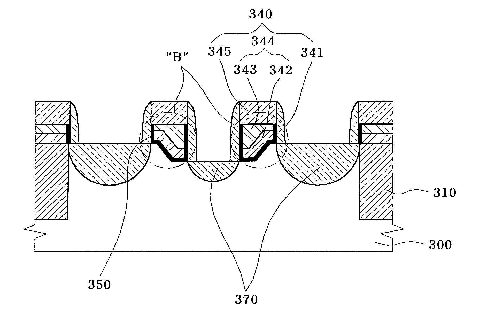
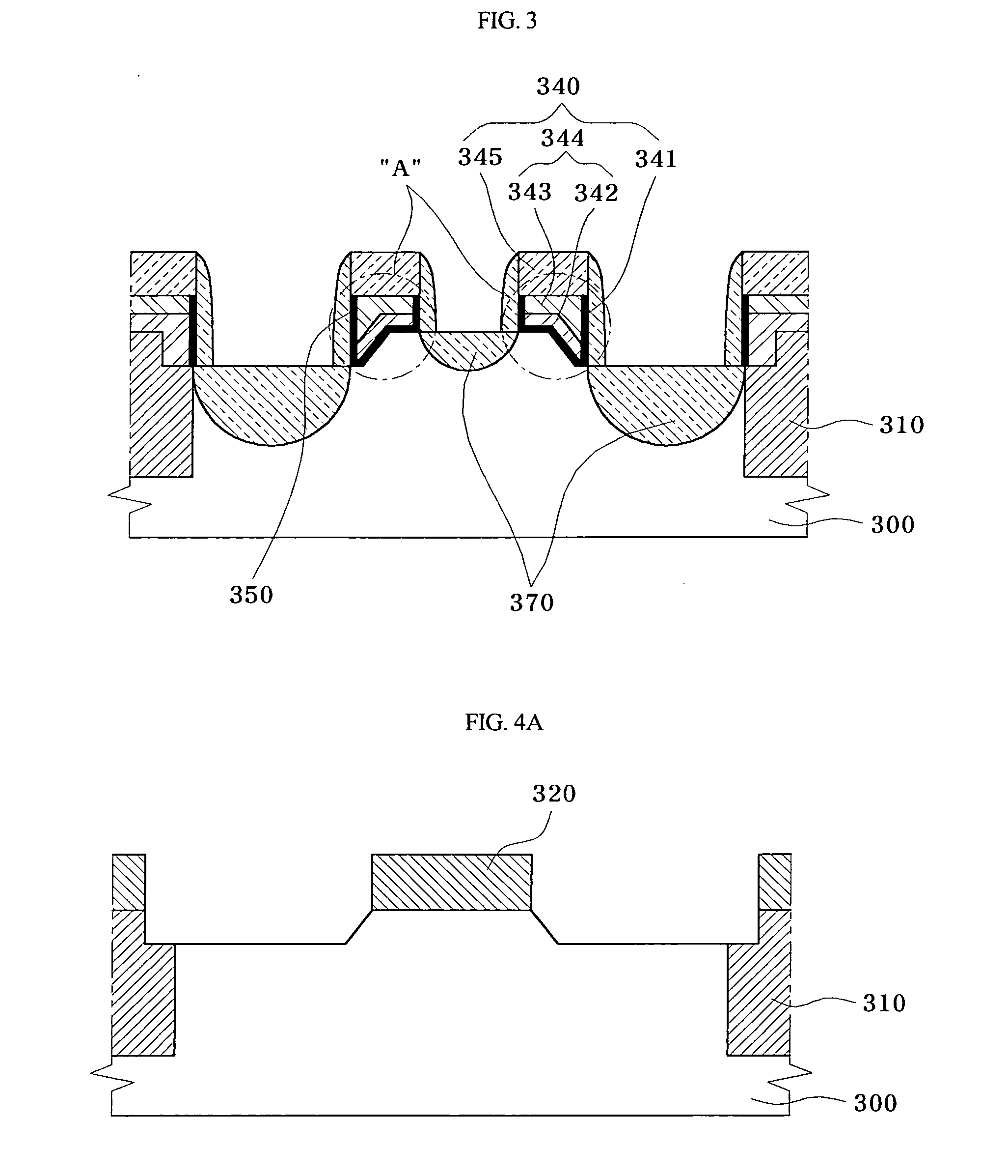
[0036]FIG. 3 is a sectional view illustrating a structure of the transistor according to the first embodiment of the present invention. FIG. 5 is a simulated electric field distribution of the transistor according to the first embodiment of the present invention.

[0037] As shown in FIG. 3, the transistor according to the first embodiment of the present invention includes a semiconductor substrate 300, which is divided into an active region and a device isolation region by a device isolation film 310. A stepped profile is formed at a portion A in the active region of the semiconductor substrate 300. The active region portion A is arranged adjacent to a storage node. The stepped profile has an upper surface, a lower surface, and a side surface extending in a substantially vertical direction. The side surface may have a height of 50 to 2,500 Å and an inclination of 10 to 90°. When the side surface has such ...

second embodiment

[0056] Hereinafter, a transistor according to the present invention will be described with reference to FIG. 6 and FIG. 3.

[0057]FIG. 6 is a sectional view illustrating a structure of the transistor according to the second embodiment of the present invention.

[0058] The structure of the transistor according to the second embodiment of the present invention shown in FIG. 6 is mainly identical to that of the first embodiment. Accordingly, the following description will be given of only the structural portion of the transistor of the second embodiment different from that of the first embodiment.

[0059] The transistor of the second embodiment is different from that of the first embodiment in terms of the positions of the upper and lower surfaces of the stepped profile. That is, in the stepped profile in the transistor according to the first embodiment, the lower surface thereof extends over the storage node and a portion of the gate formation region arranged adjacent to the storage node,...


PUM


Abstract

A transistor including a semiconductor substrate defined with an active region and a device isolation region, a gate formed on the semiconductor substrate, an insulating spacers formed on respective side walls of the gate, and source / drain junctions formed in the semiconductor substrate at opposite sides of the gate, the source / drain junctions having asymmetrical junction structures, respectively, wherein the gate has a lower portion arranged on the active region of the substrate, the lower gate portion having a stepped profile having a lower surface, an upper surface and a vertically-extending side surface. The invention also provides a method for manufacturing this transistor. In accordance with this transistor structure, an increase in the dopant concentration of a storage node is prevented. Accordingly, a reduction in the amount of leakage current is achieved, so that an improvement in the refresh characteristics of the transistor is achieved.

Description

BACKGROUND OF THE INVENTION [0001] 1. Field of the Invention [0002] The present invention relates to a semiconductor device and a method for manufacturing the semiconductor device, and, more particularly, to a transistor capable of improving the refresh characteristics of an associated cell in a dynamic random access memory (DRAM), which has a highly integrated structure including a group of cells, and a method for manufacturing the transistor. [0003] 2. Description of the Related Art [0004] A DRAM device is well known as a memory device to store data and to allow the stored date to be subsequently read out when the reading of the data is required. This DRAM device is composed of a group of cells each consisting of a capacitor to store data, that is, charge, and a transistor to perform a switching operation to discharge the charge stored in the capacitor. [0005] The data storage of the DRAM device means that charge is accumulated in the capacitors of the DRAM device. Ideally, the ch...

Claims


Application Information

Patent Timeline
Patent Type & Authority Applications(United States)
IPC IPC(8): H01L21/336H01L21/8242H01L29/10H01L29/78H01L29/788
CPCH01L27/10855H01L27/10873H01L27/10876H01L29/7834H01L29/1037H01L29/66636H01L27/10888H10B12/05H10B12/053H10B12/485H10B12/0335B42D3/10B42D5/042B42P2241/02
Inventor SUH, MOON SIK
Owner SK HYNIX INC
Why Eureka
Try Eureka