Erasable and programmable read only memory (EPROM) cell of an EPROM device and method of manufacturing a semiconductor device having the EPROM cell

a technology of erasable and programmable read only memory and semiconductor devices, which is applied in the direction of semiconductor devices, electrical devices, transistors, etc., can solve the problems of difficult to find a substitute film material, weakening of the data retention characteristic of the otp cell, etc., to and improve the data retention characteristic

Inactive Publication Date: 2007-04-10
SAMSUNG ELECTRONICS CO LTD
View PDF11 Cites 4 Cited by
  • Summary
  • Abstract
  • Description
  • Claims
  • Application Information

AI Technical Summary

Benefits of technology

[0012]The present invention provides an erasable and programmable read only memory (EPROM) device that improves a data retention characteristic of a single poly one time programmable (OTP) cell by preventing leakage of charged electrons from a floating gate. The present invention also provides a semiconductor device having a structure that improves the data retention characteristic in a single poly OTP cell region and secures a hot carrier injection (HCI) characteristic and an insulating characteristic required for forming a transistor in a main chip region. The present invention further provides a method of manufacturing a semiconductor device having a structure that improves the data retention characteristic in a single poly OTP cell region and secures the HCl characteristic and the insulating characteristic required for forming a transistor in a main chip region.

Problems solved by technology

This results in a weakening of the data retention characteristic of the OTP cell.
However, it is difficult to find a substitutable film material, which can secure a hot carrier injection (HCl) characteristic and an insulating characteristic required for forming a transistor in a main chip region, and that is formed at the same level as the SiON film on the substrate except the OTP cell region.

Method used


Image

  • Erasable and programmable read only memory (EPROM) cell of an EPROM device and method of manufacturing a semiconductor device having the EPROM cell
  • Erasable and programmable read only memory (EPROM) cell of an EPROM device and method of manufacturing a semiconductor device having the EPROM cell
  • Erasable and programmable read only memory (EPROM) cell of an EPROM device and method of manufacturing a semiconductor device having the EPROM cell

Examples


Embodiment Construction

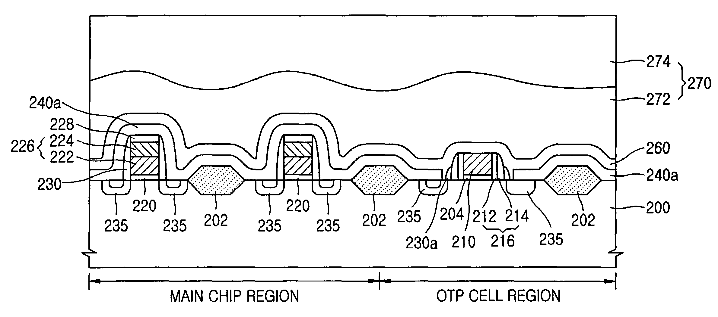
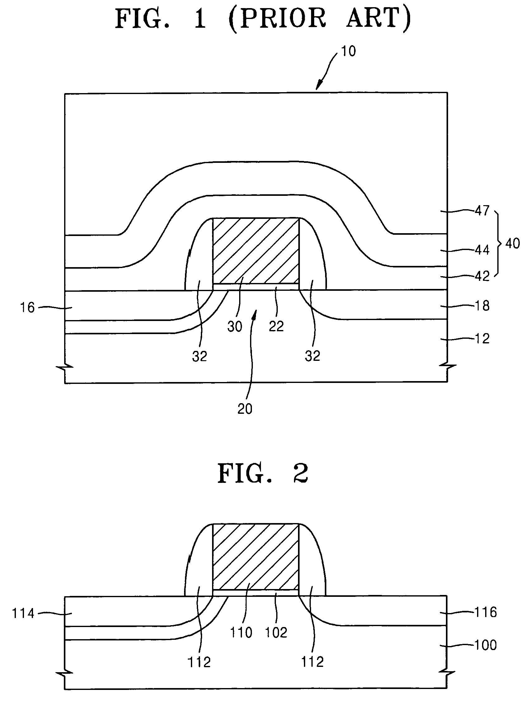
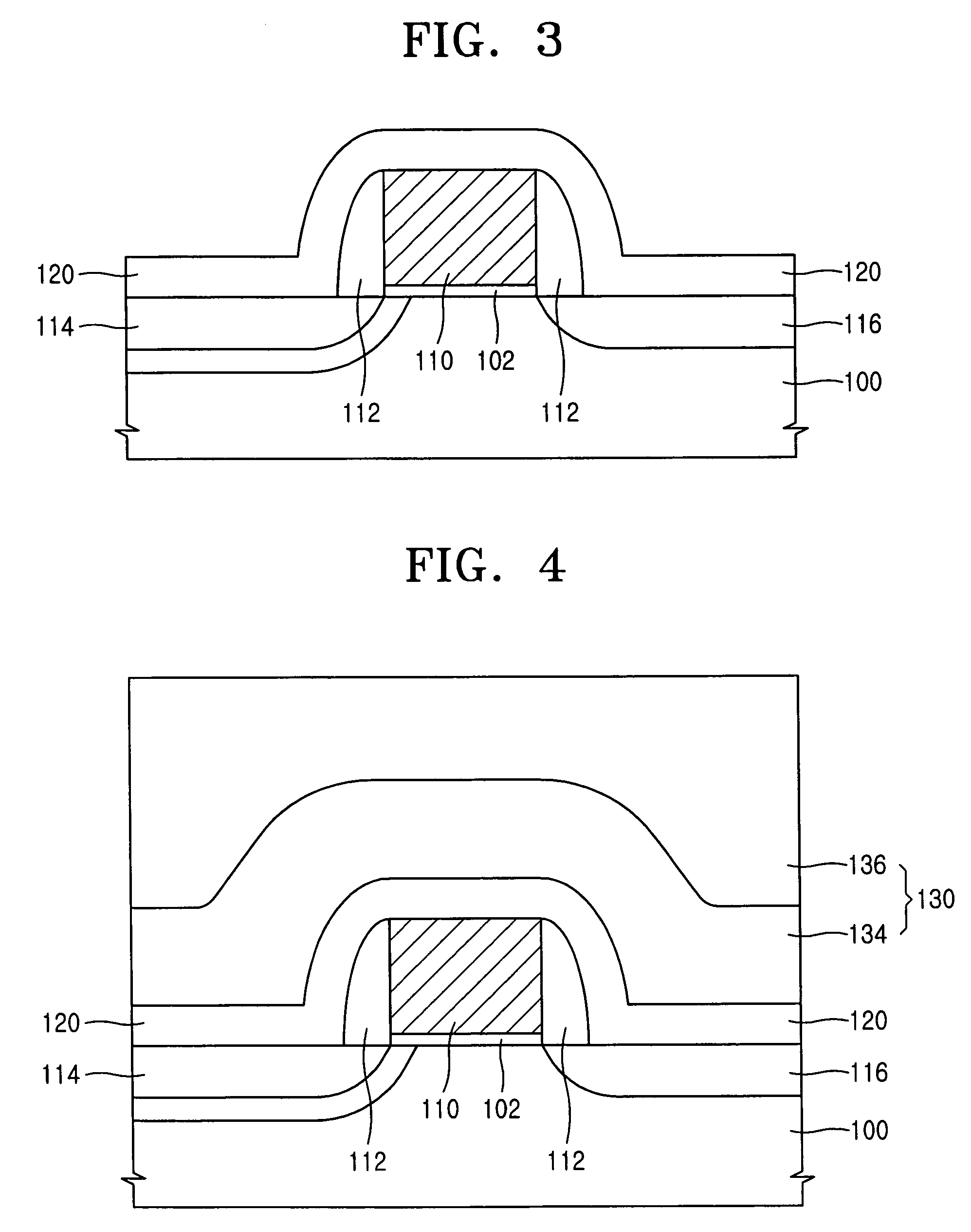
[0023]FIGS. 2 through 5 are cross-sectional views for describing a method of manufacturing a single poly one time programmable (OTP) cell of an erasable and programmable read only memory (EPROM) device, according to a preferred embodiment of the present invention.

[0024]Referring to FIG. 2, after defining active regions on a semiconductor substrate 100 by a device isolation process, a gate oxide film 102 with a thickness of approximately 140Å is formed on an OTP cell region of an active region on the substrate 100. After forming a conductive layer such as a doped polysilicon layer on the gate oxide film 102, a floating gate 110 is formed by patterning the conductive layer. After depositing an insulating film covering the entire surface of the floating gate 110, insulating spacers 112 covering sidewalls of the floating gate 110 are formed by etching back the insulating film. The insulating spacers can be formed, for example, of silicon nitride. Alternatively, the spacers can be formed...


PUM


Abstract

Provided is an erasable and programmable read only memory (EPROM) device in which a plasma enhanced oxide (PEOX) film covers an upper surface of a floating gate in a single poly one time programmable (OTP) cell and a method of manufacturing a semiconductor device having the same. The semiconductor device comprises a substrate having an OTP cell region, on which a floating gate is formed for making an OTP cell transistor, and a main chip region, on which a gate of a transistor is formed. A PEOX film is formed on the OTP cell region and the main chip region. The PEOX film covers the floating gate in a close state and covers the gate by a predetermined distance. A silicon oxy nitride (SiON) film is interposed between the gate and the PEOX film in the main chip region.

Description

[0001]This application claims priority to Korean Patent Application No. 2003-77188 filed on Nov. 1, 2003 in the Korean Intellectual Property Office, the disclosure of which is incorporated herein in its entirety by reference.BACKGROUND OF THE INVENTION[0002]1. Field of the Invention[0003]The present invention relates to a semiconductor device and a method of manufacturing the same, and more particularly, to an erasable and programmable read only memory (EPROM) device for a single poly one time programmable (OTP) cell and a method of manufacturing a semiconductor device having the same.[0004]2. Description of the Related Art[0005]An EPROM is widely used in a variety of logic devices because it can electrically store and erase data, and it can retain data when power is turned off. The EPROM is a core device of a micro controller unit for controlling equipment such as a central processing unit (CPU) and remote controllers for household appliances like televisions (TVs), video, or audio...

Claims


Application Information

Patent Timeline
Patent Type & Authority Patents(United States)
IPC IPC(8): H01L21/70H01L27/10H01L21/82H01L21/8247H01L27/115H01L29/788H01L29/792H01L29/94
CPCH01L27/115H01L27/11526H01L27/11546H10B41/40H10B69/00H10B41/49
Inventor LEE, KI-HYUNGYOO, SEUNG-HAN
Owner SAMSUNG ELECTRONICS CO LTD
Why Eureka
Try Eureka