Nonvolatile memory device and method for fabricating the same

a non-volatile memory and semiconductor technology, applied in the direction of semiconductor devices, electrical equipment, transistors, etc., can solve the problems of increasing the electric field between the source and the drain, increasing the junction leakage current, and reducing the threshold voltage (vt). , to achieve the effect of increasing the effective channel length

Inactive Publication Date: 2010-09-28
SK HYNIX INC
View PDF10 Cites 3 Cited by
  • Summary
  • Abstract
  • Description
  • Claims
  • Application Information

AI Technical Summary

Benefits of technology

[0014]Embodiments of the present invention are directed to provide a nonvolatile memory device and a method for fabricating the same, which can increase an effective channel length to secure an electric characteristic of the device.

Problems solved by technology

However, if the design rule is decreased for high-integration, the channel length of a device may shorten, causing the threshold voltage (Vt) to decrease.
However, the increased doping concentration level of the ions implanted in the substrate may cause an increased electric field between source and drain, increased junction leakage current, and a short channel effect (SCE) inducing drain induced barrier lowering (DIBL).
Thus, a short channel effect may increase, causing difficulty in highly integrating the nonvolatile memory device.

Method used


Image

  • Nonvolatile memory device and method for fabricating the same
  • Nonvolatile memory device and method for fabricating the same
  • Nonvolatile memory device and method for fabricating the same

Examples


Embodiment Construction

[0024]Embodiments of the present invention relate to a nonvolatile memory device and a method for fabricating the same.

[0025]Referring to the drawings, the illustrated thickness of layers and regions are exaggerated to facilitate explanation. When a first layer is referred to as being “on” a second layer or “on” a substrate, it could mean that the first layer is formed directly on the second layer or the substrate, or it could also mean that a third layer may exist between the first layer and the substrate. Furthermore, the same or like reference numerals throughout the various embodiments of the present invention represent the same or like elements in different drawings.

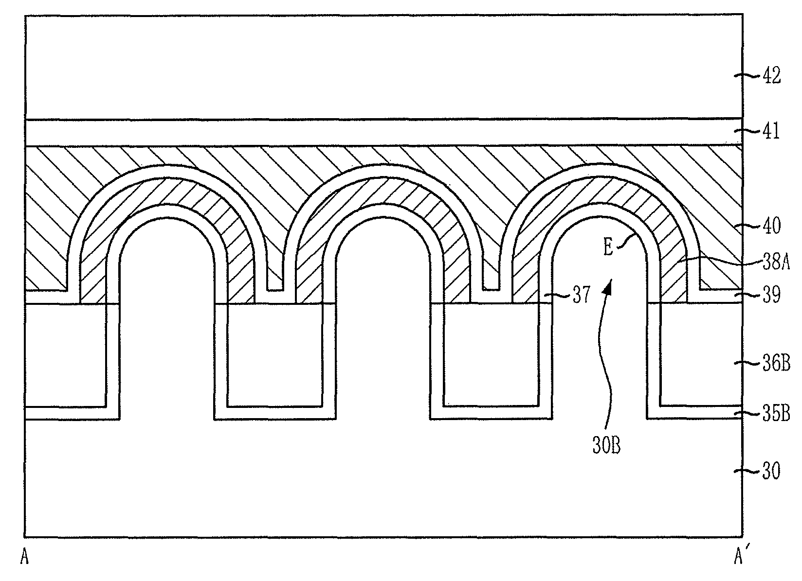
[0026]FIG. 4 illustrates a top view of a nonvolatile memory device in accordance with an embodiment of the present invention. FIG. 5 illustrates a cross-sectional view of the nonvolatile memory device shown in FIG. 4 in accordance with a line A-A′. FIG. 6 illustrates a cross-sectional view of the nonvolatile memory ...


PUM


Abstract

A nonvolatile memory device includes a control gate formed along a first direction over a substrate, an active region formed over the substrate, the active region being defined along a second direction crossing the control gate and including a fin type protruding portion having rounded top corners at a region where the control gate and the active region overlap, a floating gate formed over a surface of the protruding portion of the active region below the control gate and formed to a substantially uniform thickness along the surface profile of the protruding portion of the active region, a tunneling insulation layer formed between the floating gate and the active region, and a dielectric layer formed between the floating gate and the control gate.

Description

CROSS-REFERENCE TO RELATED APPLICATIONS[0001]The present invention claims priority of Korean patent application number 2007-0045015, filed on May 9, 2007, which is incorporated by reference in its entirety.BACKGROUND OF THE INVENTION[0002]The present invention relates to a method for fabricating a semiconductor device, and more particularly, to a method for fabricating a nonvolatile memory device.[0003]Recently, research on high-integration memory device technology has been actively conducted to develop high capacity memory devices which can electrically program and erase, and store a large amount of data. However, if the design rule is decreased for high-integration, the channel length of a device may shorten, causing the threshold voltage (Vt) to decrease.[0004]Thus, the doping concentration level of threshold voltage adjusting ions has to be increased to compensate the lowered threshold voltage. However, the increased doping concentration level of the ions implanted in the substr...

Claims


Application Information

Patent Timeline
Patent Type & Authority Patents(United States)
IPC IPC(8): H01L21/762H01L27/088
CPCH01L27/115H01L27/11521H10B69/00H10B41/30H01L21/02362H01L21/31051H01L21/76838
Inventor KIM, JAE-HONG
Owner SK HYNIX INC
Why Eureka
Try Eureka