(Al, Ga, In) N-based compound semiconductor and method of fabricating the same

Inactive Publication Date: 2007-04-05
SEOUL OPTO DEVICE CO LTD
View PDF39 Cites 4 Cited by
  • Summary
  • Abstract
  • Description
  • Claims
  • Application Information

AI Technical Summary

Benefits of technology

[0021] According to the present invention, there are provided a (Al, Ga, In) N-based compound semiconductor device and a method of fabricating the same, wherein P type conductivity can be sufficiently secured and good ohmic contact characteristics can be obtained without performing a conventional annealing process. And, according to the present invention, there are provided a P layer of a (Al, Ga, In) N-based compound semiconductor and a method of f

Problems solved by technology

However, the P type impurities, e.g., magnesium (Mg), do not fulfill the function as an electron acceptor that provides free holes, since they are easily bonded with hydrogen (H) existing in a growth chamber.
However, the annealing process has a problem in that it makes a fabrication process of a compound semiconductor device complicated

Method used


Image

  • (Al, Ga, In) N-based compound semiconductor and method of fabricating the same
  • (Al, Ga, In) N-based compound semiconductor and method of fabricating the same
  • (Al, Ga, In) N-based compound semiconductor and method of fabricating the same

Examples


Embodiment Construction

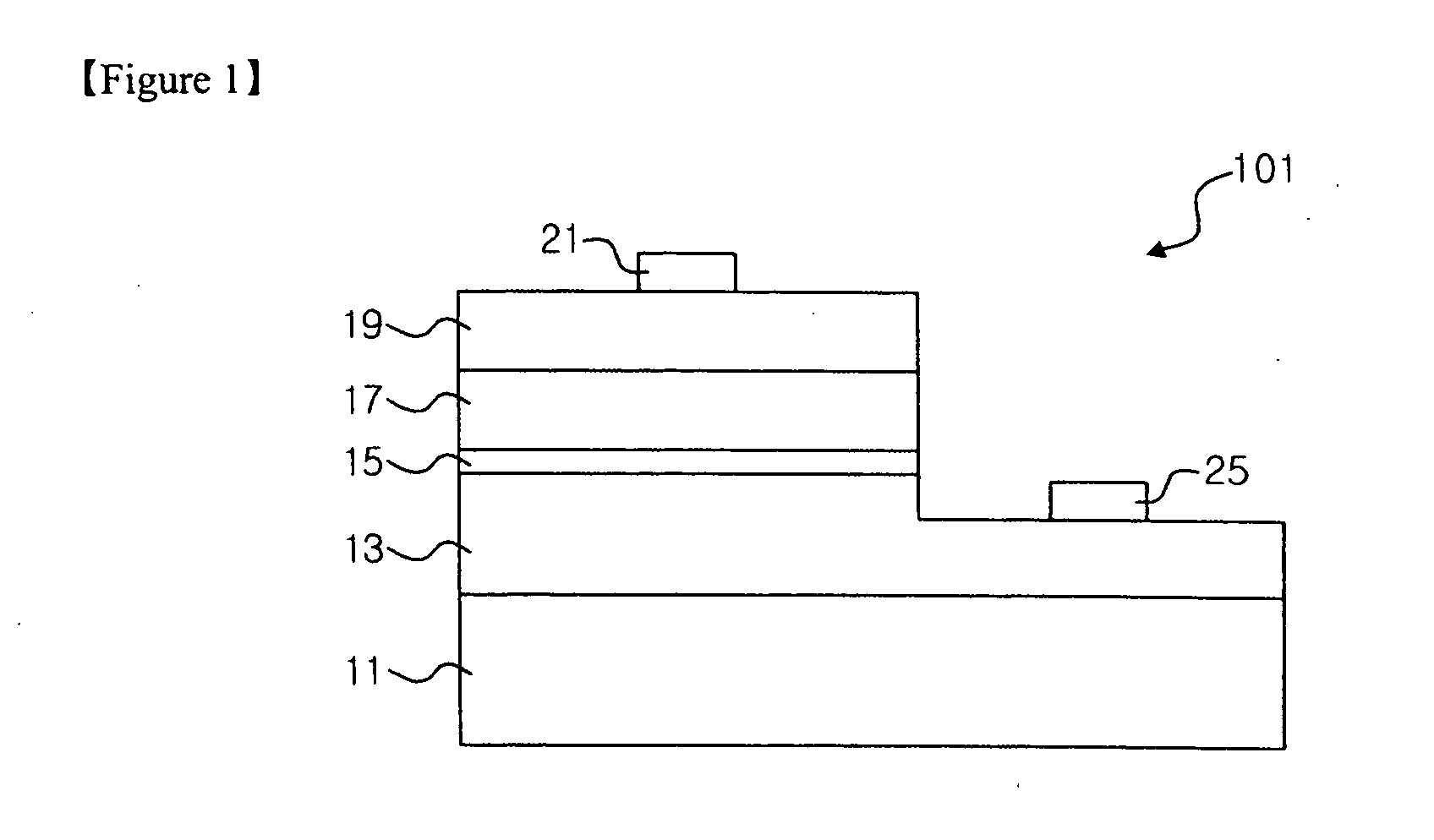
[0030]1: (Al, Ga, In) N-based compound semiconductor device, 11: Substrate,

[0031]12: Buffer layer, 13: N layer,

[0032]15: Active layer, 17: P layer,

[0033]25: (Al, Ga, In) N-based compound semiconductor layer, 27: Epi,

[0034]31, 35: Electrode

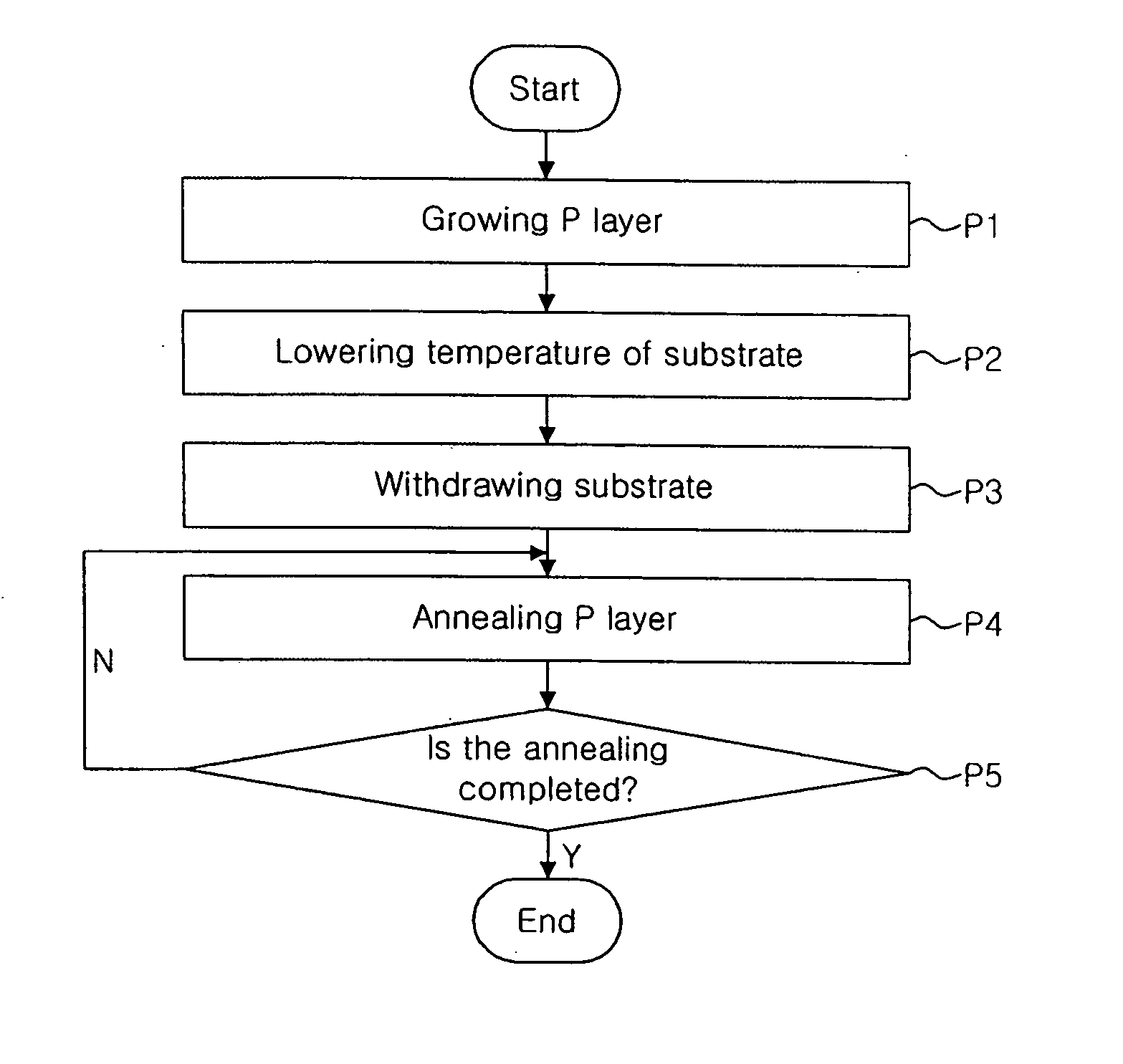
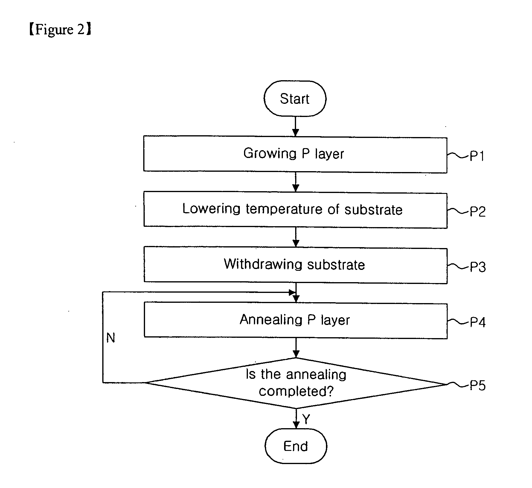
[0035] Hereinafter, a (Al, Ga, In) N-based compound semiconductor and a method of fabricating the same will be described in detail according to the present invention with reference to the accompanying drawings.

[0036]FIG. 3 is a perspective view of a (Al, Ga, In) N-based compound semiconductor device comprising a P layer and an electrode according to an embodiment of the present invention, and FIG. 4 is a cross-sectional view of FIG. 3. The (Al, Ga, In) N-based compound semiconductor device 1 comprises a substrate 11, (Al, Ga, In) N-based compound semiconductor layers 25 grown on the substrate 11, and electrodes 31 and 35 formed on the (Al, Ga, In) N-based compound semiconductor layers 25. Meanwhile, an electrode pad 33 for electrical connecti...


PUM


Abstract

Disclosed are a (Al, Ga, In) N-based compound semiconductor device and a method of fabricating the same. The (Al, Ga, In) N-based compound semiconductor device of the present invention comprises a substrate; a (Al, Ga, In) N-based compound semiconductor layer grown on the substrate; and an electrode formed of at least one material or an alloy thereof selected from the group consisting of Pt, Pd and Au on the (Al, Ga, In) N-based compound semiconductor layer. Further, the method of fabricating the (Al, Ga, In) N-based compound semiconductor device comprises the steps of growing a P layer including P type impurities in a growth chamber; discharging hydrogen and a hydrogen source gas in the growth chamber; lowering the temperature of the (Al, Ga, In) N-based compound semiconductor with the P layer formed thereon to such an extent that it can be withdrawn to the outside from the growth chamber; withdrawing the (Al, Ga, In) N-based compound semiconductor from the growth chamber; and forming an electrode of at least one material or an alloy thereof selected from the group consisting of Pt, Pd and Au on the P layer. According to the present invention, it is possible to sufficiently secure P type conductivity and obtain good ohmic contact characteristics without performing an annealing process. And, no ftrther annealing is necessary when Pt, Pd, Au electrode are used.

Description

BACKGROUND OF THE INVENTION [0001] The present invention relates to Aluminum (Al), Gallium (Ga), Indium (In) N-based compound semiconductor device and a method of fabricating the same, and more particularly, to a (Al, Ga, In) N-based compound semiconductor device comprising a (Al, Ga, In) N-based compound semiconductor layer (P layer) including P type impurities and a transparent electrode provided on the P layer, and a method of fabricating the (Al, Ga, In) N-based compound semiconductor device. [0002] A (Al, Ga, In) N-based compound semiconductor is applied, for example, to a compound semiconductor device such as a light emitting diode (LED) or a laser diode (LD). FIG. 1 is a cross-sectional view schematically showing a conventional (Al, Ga, In) N-based compound semiconductor device. [0003] Referring to FIG. 1, a (Al, Ga, In) N-based compound semiconductor layer (N layer) 13 including N type impurities, an active layer 15 and a (Al, Ga, In) N-based compound semiconductor layer (P ...

Claims


Application Information

Patent Timeline
IPC IPC(8): C30B23/00C30B25/00C30B28/12C30B28/14H01L33/06H01L33/32H01L33/34H01L33/40
CPCH01L33/0095H01L33/40H01L33/32
Inventor LEE, CHUNG
Owner SEOUL OPTO DEVICE CO LTD
Why Eureka
Try Eureka