P-N junction-type compoud semiconductor light-emitting diode

A technology of light-emitting diodes and nitride semiconductors, applied in semiconductor lasers, semiconductor devices, lasers, etc., can solve the problems of inconvenient emission absorption light-emitting devices, and achieve the effect of excellent reverse breakdown voltage

Inactive Publication Date: 2007-05-23
SHOWA DENKO KK
View PDF1 Cites 3 Cited by
  • Summary
  • Abstract
  • Description
  • Claims
  • Application Information

AI Technical Summary

Problems solved by technology

Therefore, it cannot transmit the blue or green band emission through
Attempts to use a conventional BP layer with a narrow bandgap as a contact layer and arrange it to direct the emission to the outside only lead to the absorption of the emission and the inconvenience of obtaining a high-brightness light-emitting device

Method used


Image

  • P-N junction-type compoud semiconductor light-emitting diode
  • P-N junction-type compoud semiconductor light-emitting diode
  • P-N junction-type compoud semiconductor light-emitting diode

Examples


example

[0041] Hereinafter, the present invention will be specifically described by citing an example of manufacturing a pn junction type compound semiconductor LED using a single boron phosphide semiconductor layer formed on a p-type gallium nitride (GaN) layer as an example.

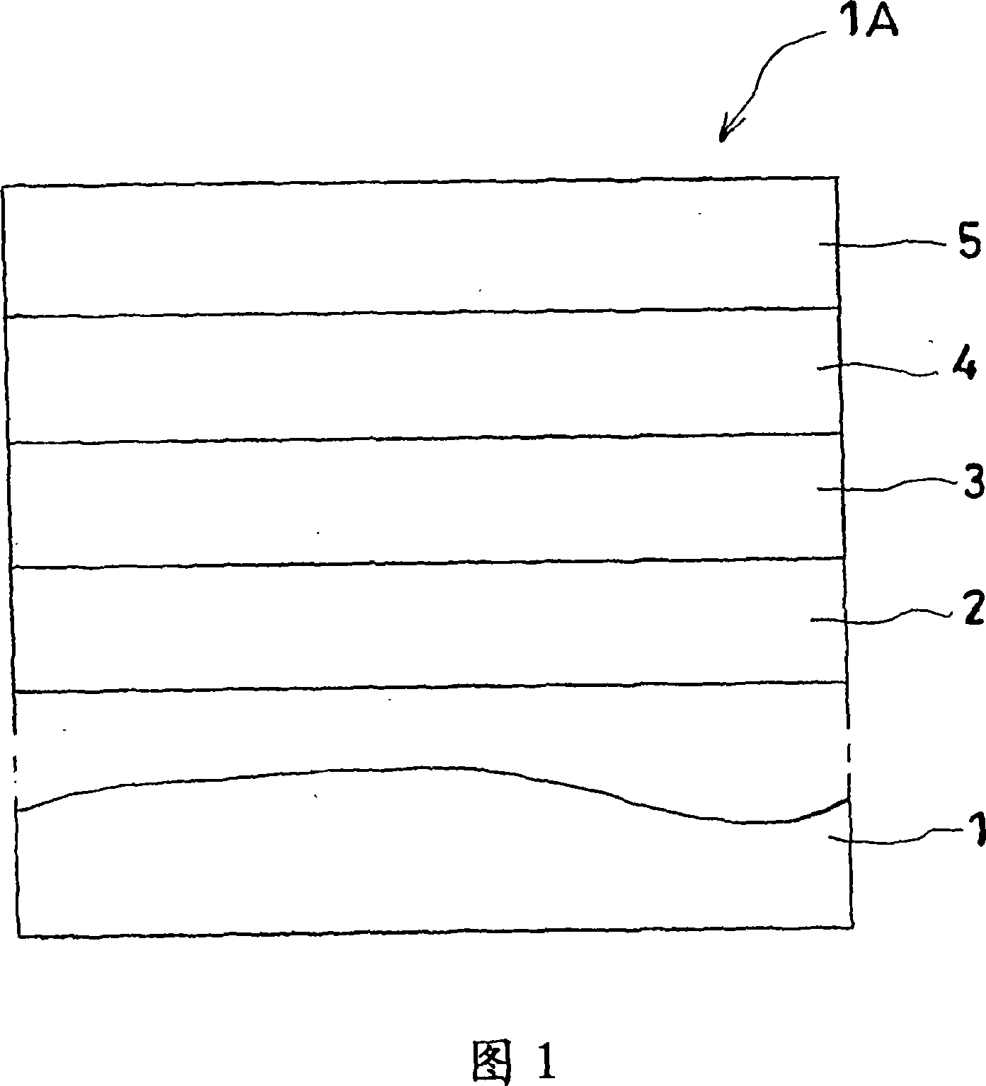
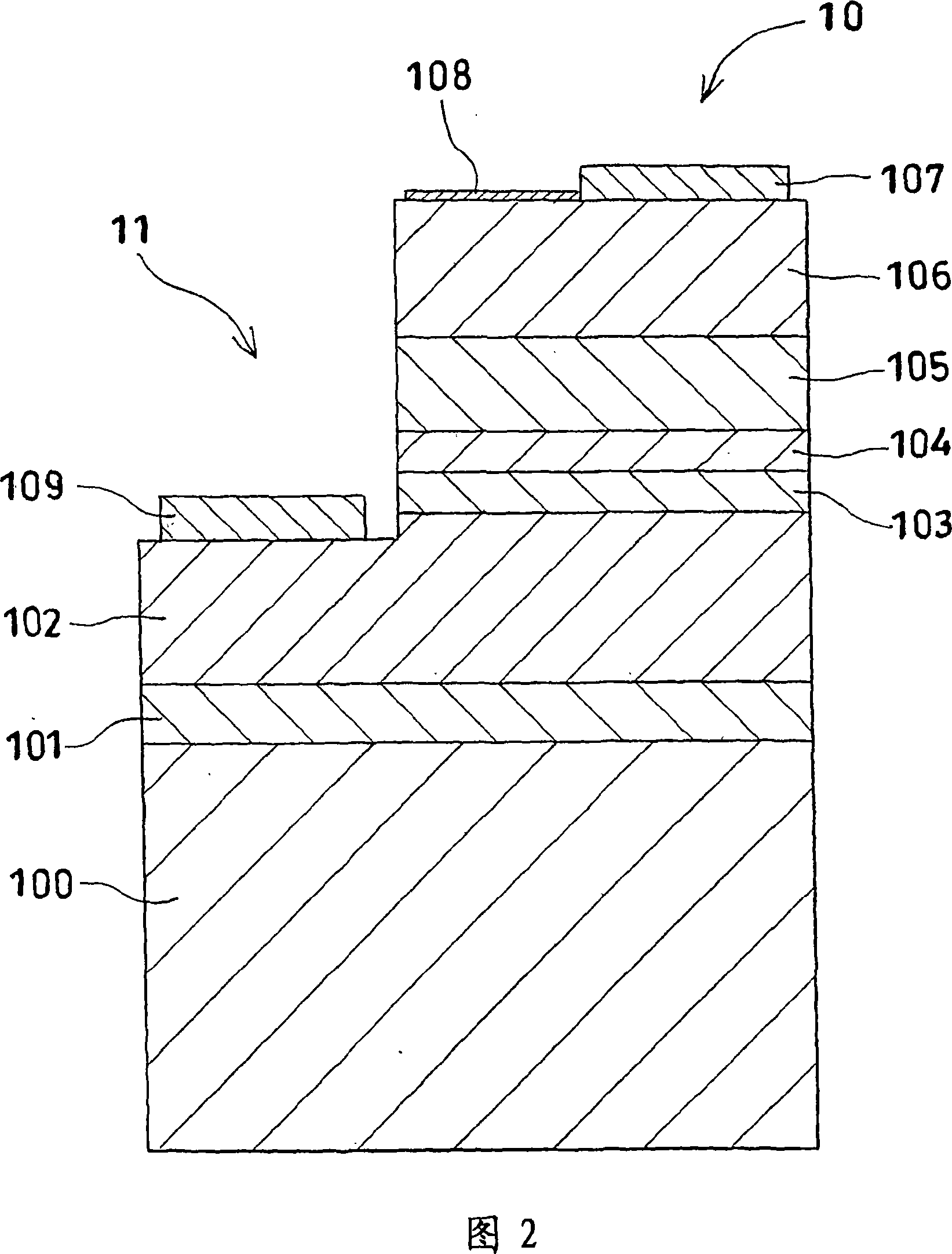
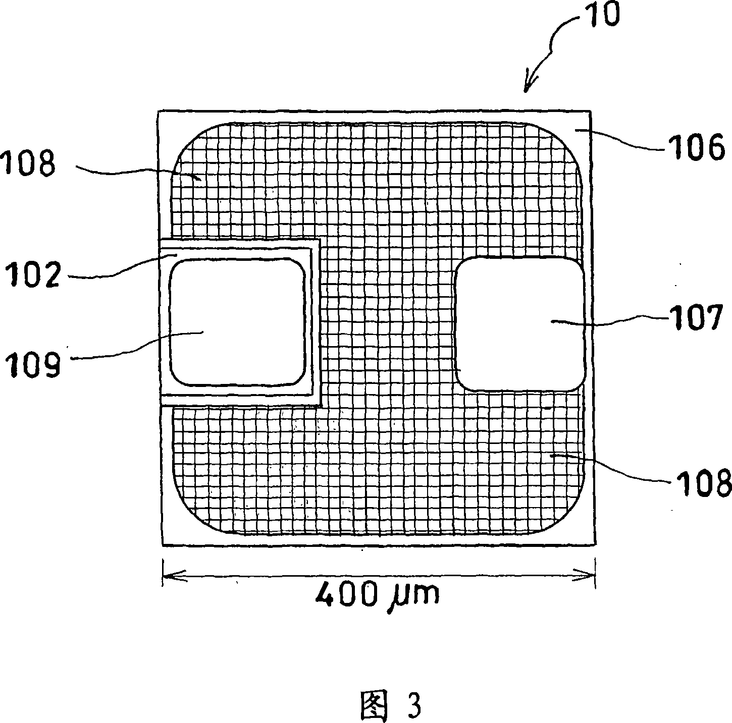
[0042] Fig. 2 schematically shows a cross-sectional view of a stack structure 11 for manufacturing an LED 10 having a double hetero (DH) junction structure. FIG. 3 shows a schematic plan view of the LED 10 .

[0043] Through the (0001) sapphire (α-Al 2 o 3On a single crystal) substrate 100, an undoped buffer layer 101 formed of GaN and a lower cladding layer 102 formed of n-type GaN doped with silicon (Si) are sequentially stacked in the following order (n=7×10 18 cm -3 , layer thickness (t) = 3μm), containing undoped n-type Ga 0.86 In 0.14 N-layer light emitting layer 103, p-type Al doped with Mg 0.06 Ga 0.94 The upper cladding layer (group III nitride semiconductor layer) 104 (p=3×10) formed of N 17 ...


PUM


Abstract

In a p-n junction-type compound semiconductor light-emitting diode provided on a crystal substrate with at least an n-type active layer formed of a Group III nitride semiconductor as a light emitting layer, and with a Group III nitride semiconductor layer containing a p-type impurity on the n-type active layer, the diode has a boron phosphide-based Group III-V compound semiconductor layer possessing a band gap exceeding that of the Group III nitride semiconductor forming the n-type active layer at room temperature and exhibiting a p-type electroconductivity in an undoped state deposited on the p-type impurity-containing Group Ill nitride semiconductor layer, and has an ohmic positive electrode joined to a surface of the boron phosphide-based Group III-V compound semiconductor layer.

Description

[0001] Cross References to Related Applications [0002] This application is based on an application filed at 35 U.S.C. §111(a) under 35 U.S.C. §119(e)(1), claiming to be based on provisional application 60 / 572,268 filed May 19, 2004 under 35 U.S.C. §111(b) and priority of Japanese Patent Application No. 2004-137229 filed May 6, 2004. technical field [0003] The present invention relates to a pn junction type compound semiconductor light-emitting diode arranged on a crystal substrate, which has at least an n-type active (light-emitting) layer formed of a III-group nitride semiconductor and an n-type active layer containing p on the n-type active layer. Type III nitride semiconductor layer with impurities. Background technique [0004] As a light-emitting device that mainly emits blue to green light, a light-emitting diode (LED) used as a III-V group compound semiconductor (III-nitride semiconductor) layer containing, for example, nitrogen (N) as a group V constituent eleme...

Claims


Application Information

Patent Timeline
Patent Type & Authority Applications(China)
IPC IPC(8): H01L33/00H01L33/26H01L33/32H01S5/042H01S5/30H01S5/323
CPCH01L33/26H01L33/32H01S5/32341H01S5/3054H01S5/0421
Inventor 小田原道哉宇田川隆
Owner SHOWA DENKO KK
Why Eureka
Try Eureka