Organic light emitting device having transparent electrode where conducting filaments formed and method of manufacturing the same

a light emitting device and organic technology, applied in the field of organic light emitting devices, can solve the problems of low light extraction efficiency, low charge injection efficiency, and inability to easily implement traditional light sources, and achieve good ohmic contact characteristics, high transmittance, and high transmittance

Active Publication Date: 2017-02-14
KOREA UNIV RES & BUSINESS FOUND
View PDF20 Cites 3 Cited by
  • Summary
  • Abstract
  • Description
  • Claims
  • Application Information

AI Technical Summary

Benefits of technology

[0028]According to the present invention, a transparent electrode of an organic light emitting device is formed by using a resistance change material which has high transmittance with respect to light in a UV wavelength range and of which resistance state is to be changed from a high resistance state into a low resistance state due to conducting filaments, which current can flow through, formed in the material if a voltage exceeding a threshold voltage inherent in a material is applied to the material, so that it is possible to obtain the transparent electrode having high transmittance with respect to light in a UV wavelength range as well as light in a visible wavelength range generated by the organic light emitting device and having high conductivity due to good ohmic contact characteristic with respect to an organic material layer constituting an organic semiconductor layer, and thus, it is possible to decrease a driving voltage.
[0029]In addition, according to the present invention, a current spreading layer formed by using CNT or graphene having good ohmic contact characteristic and high transmittance is formed on an upper or lower portion of a transparent electrode to connect conducting filaments formed in the transparent electrode, so that current flowing into the transparent electrode is allowed to spread through the entire organic material layer, and thus, it is possible to prevent the problem of current concentration from occurring.

Problems solved by technology

In particular, unlike the LED as a point light source, the OLED has a structure of thin planar light source, so that it is possible to implement transparent and flexible illumination, which cannot be easily implemented in the traditional light sources.
However, in the current OLED, due to a large difference in work function between ITO (4.3 eV) mainly used for a transparent electrode and an organic semiconductor (6.3 eV), the ohmic characteristic is bad, so that there is a problem in that charge injection efficiency is low.
In addition, since ITO has large transmission loss in a UV wavelength range, in the current organic UV-LED, there is a problem in that light extraction efficiency is low.
Namely, since a material having high transmittance in a UV wavelength range has a large band gap, the conductivity thereof is too low to be used as an electrode, and since the material is not in ohmic contact with a semiconductor material, it is impossible to use the above material as an electrode.
In the related art, a transparent electrode having high transmittance with respect to light in a UV wavelength range as well in a visible wavelength range and high conductivity due to good ohmic contact cannot be implemented.

Method used


Image

  • Organic light emitting device having transparent electrode where conducting filaments formed and method of manufacturing the same
  • Organic light emitting device having transparent electrode where conducting filaments formed and method of manufacturing the same
  • Organic light emitting device having transparent electrode where conducting filaments formed and method of manufacturing the same

Examples


first embodiment

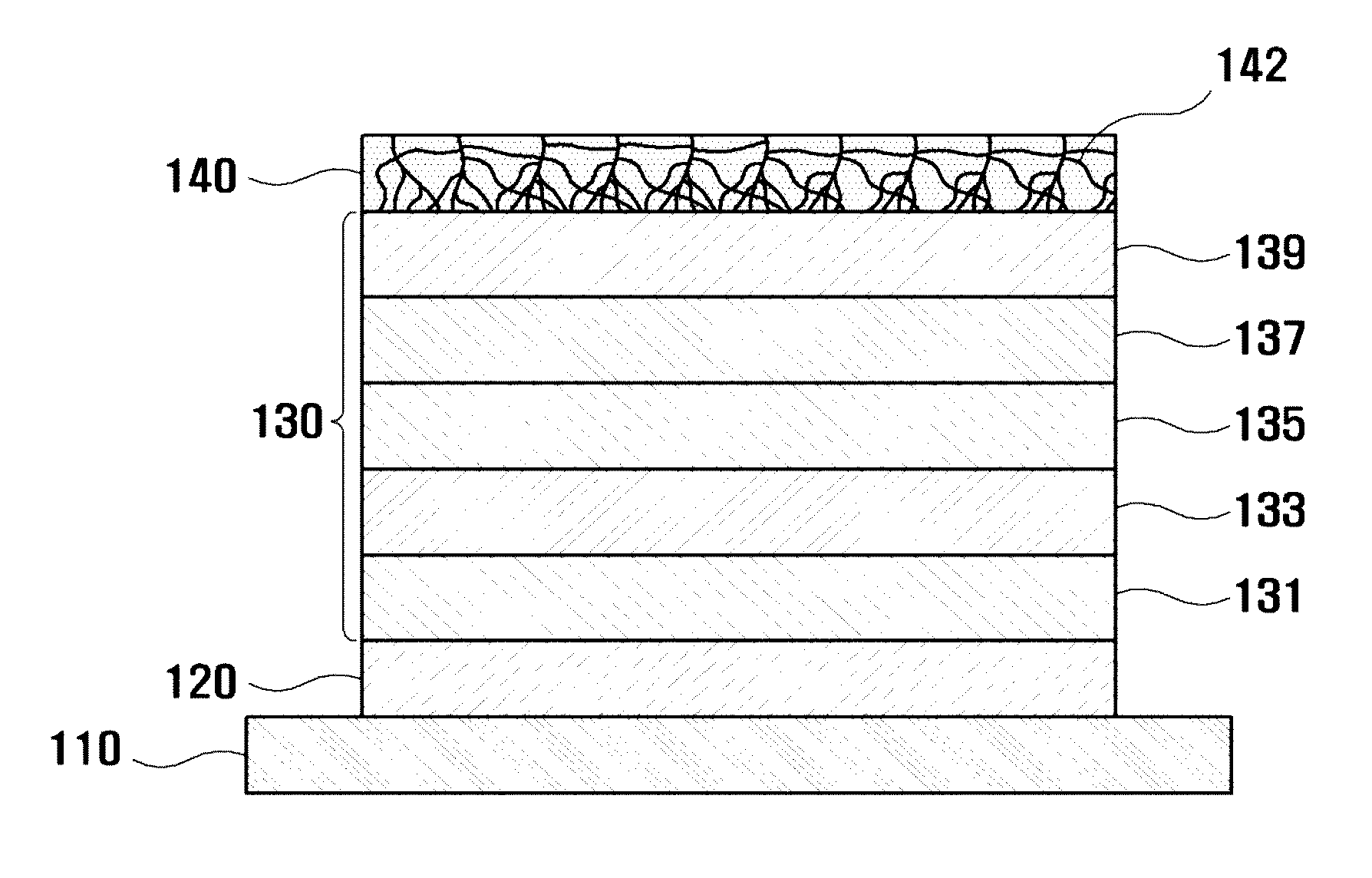
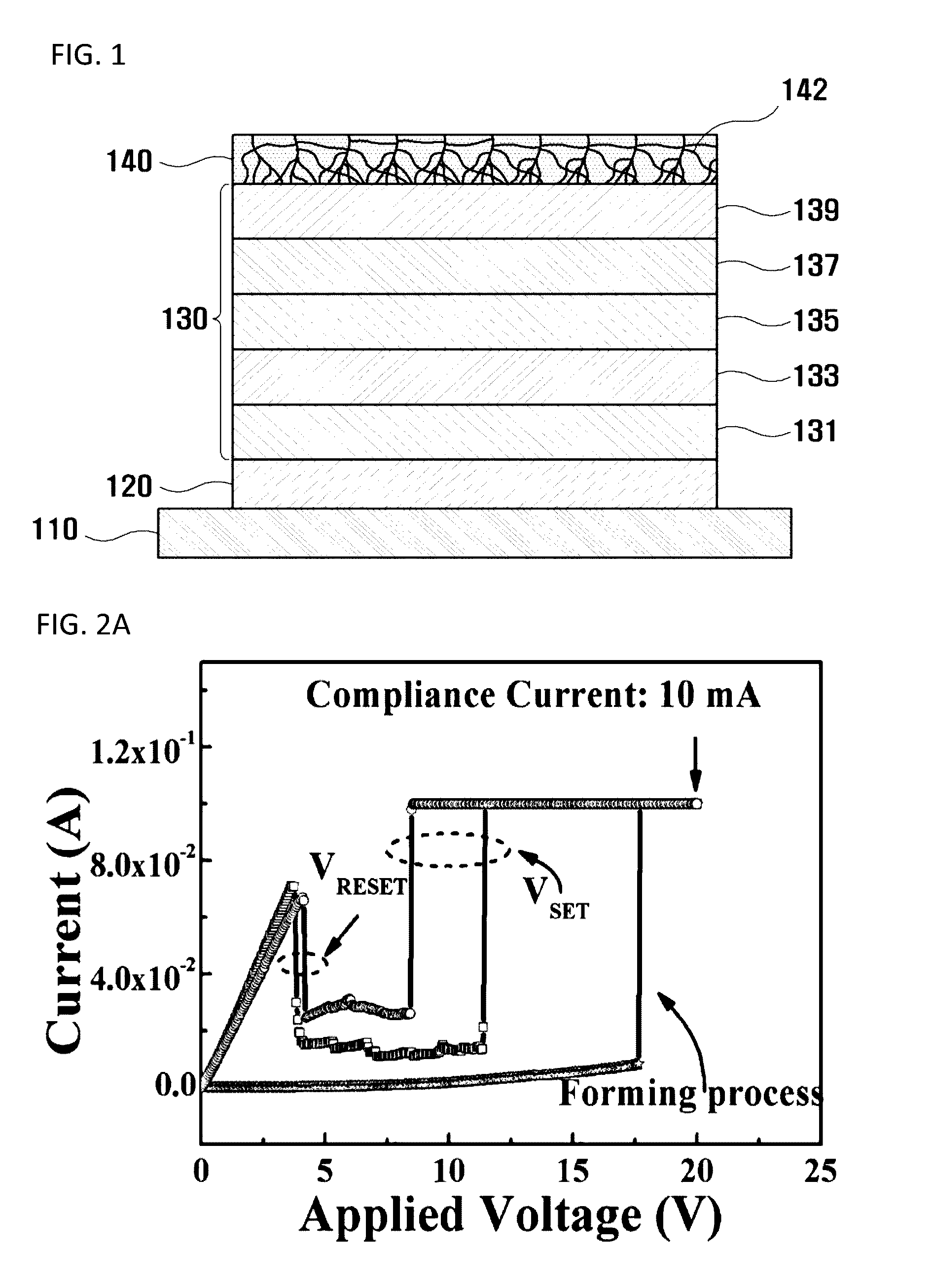
[0039]FIG. 1 is a diagram illustrating a configuration of an organic light emitting device including a transparent electrode 140 according to the present invention.

[0040]Referring to FIG. 1, an organic light emitting device according to the first embodiment of the present invention is a top-emission type organic light emitting device. In the organic light emitting device, a second electrode 120 and an organic material layer 130 including a light emitting layer 135 are sequentially formed on a substrate 110, and the organic material layer 130 is configured by sequentially forming a hole injection layer 131, a hole transport layer 133, the light emitting layer 135, an electron transport layer 137, and an electron injection layer 139. Hereinafter, the case where the organic material layer 130 includes the hole injection layer 131 to the electron injection layer 139 will be described as an example. The configurations from the substrate 110 to the electron injection layer 139 may be the ...

second embodiment

[0064]FIG. 5 is a diagram illustrating a configuration of an organic light emitting device including a transparent electrode 540 according to the present invention.

[0065]Referring to FIG. 5, an organic light emitting device according to the second embodiment of the present invention is a bottom-emission type organic light emitting device. In the organic light emitting device, a first electrode 540 (hereinafter, referred to as a “transparent electrode”) is formed on a substrate 510 constructed with a transparent glass or a transparent plastic material, and an organic material layer 530 including a light emitting layer 535 and a second electrode 520 are sequentially formed on the transparent electrode 540. The organic material layer 530 can be configured by sequentially forming a hole injection layer 531, a hole transport layer 533, a light emitting layer 535, an electron transport layer 537, and an electron injection layer 539. Hereinafter, the configuration will be described as an e...


PUM


Abstract

Provided is an organic light emitting device including a transparent electrode in which conducting filaments are formed and a method of manufacturing the same. In the organic light emitting device, a transparent electrode of an organic light emitting device is formed by using a resistance change material which has high transmittance with respect to light in a UV wavelength range and of which resistance state is to be changed from a high resistance state into a low resistance state due to conducting filaments, which current can flow through, formed in the material if a voltage exceeding a threshold voltage inherent in a material is applied to the material, so that it is possible to obtain the transparent electrode having high transmittance with respect to light in a UV wavelength range as well as light in a visible wavelength range generated by the organic light emitting device and having high conductivity.

Description

BACKGROUND OF THE INVENTION[0001]1. Field of the Invention[0002]The present invention relates to an organic light emitting device and a method of manufacturing the organic light emitting device, and more particularly, to an organic light emitting device including a transparent electrode having good ohmic contact characteristic and high transmittance and a method of manufacturing the organic light emitting device.[0003]2. Description of the Related Art[0004]Recently, in response to the government's low-carbon green growth policy stance, semiconductor illumination using LEDs (light emitting diodes) and OLEDs (organic light emitting diodes) as semiconductor light sources has attracted much attention. The semiconductor illumination is environment-friendly illumination which does not use hazardous substances such as mercury and lead, and the semiconductor illumination is also low-power-consumption illumination of which power efficiency is much higher than that of traditional illumination...

Claims


Application Information

Patent Timeline
Patent Type & Authority Patents(United States)
IPC IPC(8): H01L51/52H01L51/10H01L51/05H01L51/56H05B33/26B82Y10/00H01L51/50H01L51/00
CPCH01L51/5215B82Y10/00H01L51/0591H01L51/102H01L51/5012H01L51/5056H01L51/5072H01L51/5088H01L51/5092H01L51/5212H01L51/5234H01L51/56H05B33/26H01L51/0048H01L51/52H01L2251/301H01L2251/305H01L2251/308H10K85/221H10K10/50H10K10/82H10K50/80H10K50/814H10K50/816H10K50/828H10K2102/101H10K2102/00H10K2102/103H10K50/81H10K50/84H10K50/858H10K50/11H10K50/15H10K50/16H10K50/17H10K50/171H10K71/00
Inventor KIM, TAE GEUNKIM, HEE-DONG
Owner KOREA UNIV RES & BUSINESS FOUND
Why Eureka
Try Eureka