Silicon carbide PiN device ohmic contact method

An ohmic contact, silicon carbide technology, applied in semiconductor devices, semiconductor/solid-state device manufacturing, electrical components, etc., can solve problems affecting the performance of silicon carbide PiN devices, deterioration of N-type ohmic contact quality, etc., to achieve good ohmic contact characteristics, The effect of simplifying the process flow

Active Publication Date: 2016-01-13
ZHUZHOU CRRC TIMES SEMICON CO LTD
View PDF6 Cites 3 Cited by
  • Summary
  • Abstract
  • Description
  • Claims
  • Application Information

AI Technical Summary

Problems solved by technology

In this method, the N-type ohmic contact actually undergoes two annealing processes, which will lead to the deterioration of the quality of the N-type ohmic contact, which will seriously affect the performance of SiC PiN devices.

Method used


Image

  • Silicon carbide PiN device ohmic contact method
  • Silicon carbide PiN device ohmic contact method
  • Silicon carbide PiN device ohmic contact method

Examples


Embodiment 1

[0056] Prepare the SiC PiN substrate

[0057] The SiC epitaxial wafer of NORSTEL Company is purchased as the silicon carbide PiN substrate used in the present invention. The SiC epitaxial wafer includes an N-type SiC substrate, an N-type SiC epitaxial layer and a P-type SiC epitaxial layer in sequential contact, wherein the thickness of the N-type SiC substrate is 350 μm±25 μm, and the resistivity is 15-25mΩ·cm; N The doping concentration of the type epitaxial layer is 3E15cm -3 ; The thickness of the P-type epitaxial layer is 1 μm, and the doping concentration is 2E18cm -3 .

Embodiment 2

[0059] Fabrication of Silicon Carbide PiN Devices Forming Ohmic Contacts

[0060] 1), substrate P-type SiC epitaxial layer protection:

[0061] A low-pressure chemical vapor deposition (LPCVD) method is used to epitaxially grow an amorphous silicon layer with a thickness of 10 nm on the surface of the P-type SiC epitaxial layer of the silicon carbide PiN substrate described in Example 1. Among them, the temperature of epitaxial growth is 400-415°C, the pressure of epitaxial growth is 200-225mtorr, and the reaction gas used for epitaxial growth is SiH 4 , the carrier gas is N 2 .

[0062] 2), the surface treatment of the base N-type SiC substrate before metal sputtering:

[0063] According to HF:H 2 The mass ratio of O=1:5 will be HF and H 2 O mixed to obtain the pickling solution; the silicon carbide PiN substrate treated in step 1) was placed in a standard flower basket, and the flower basket was placed in the pickling solution, requiring the pickling solution to complet...

Embodiment 3

[0075] 1), substrate P-type SiC epitaxial layer protection:

[0076] A low-pressure chemical vapor deposition (LPCVD) method is used to epitaxially grow an amorphous silicon layer with a thickness of 15 nm on the surface of the P-type SiC epitaxial layer of the silicon carbide PiN substrate described in Example 1. Among them, the temperature of epitaxial growth is 500-525°C, the pressure of epitaxial growth is 250-275mtorr, and the reaction gas used for epitaxial growth is SiH 4 , the carrier gas is N 2 .

[0077] 2), the surface treatment of the base N-type SiC substrate before metal sputtering:

[0078] According to HF:H 2 The mass ratio of O=1:6 will be HF and H 2 O mixed to obtain the pickling solution; the silicon carbide PiN substrate treated in step 1) was placed in a standard flower basket, and the flower basket was placed in the pickling solution, requiring the pickling solution to completely immerse the wafer, and gently shaking the flower basket, The time is 15...


PUM

PropertyMeasurementUnit
thicknessaaaaaaaaaa
electrical resistivityaaaaaaaaaa
thicknessaaaaaaaaaa

Abstract

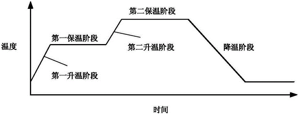
The invention belongs to the field of PiN devices, and particularly relates to a silicon carbide PiN device ohmic contact method. The method comprises the following steps that a) a silicon carbide PiN base body is prepared; b) an amorphous silicon layer is deposited on the surface of the P-type SiC epitaxial layer of the silicon carbide PiN base body; c) a metal layer is respectively deposited on the surface, on which the amorphous silicon layer is deposited, of the SiC substrate of the silicon carbide PiN base body and the surface of the amorphous silicon layer; and d) annealing processing is performed on the silicon carbide PiN base body on which the metal layer is deposited so that a silicon carbide PiN device with formation of ohmic contact is obtained, wherein annealing processing includes a first temperature rising period, a first heat preservation period, a second temperature rising period and a second heat preservation period, and temperature of the first heat preservation period and the second heat preservation period is respectively 450-550 DEG C and 970-1020 DEG C. According to the method, P-type ohmic contact and N-type ohmic contact can be formed on the silicon carbide PiN base body on which the metal layer is deposited through one time of annealing process.

Description

technical field [0001] The invention belongs to the field of PiN devices, in particular to an ohmic contact method for silicon carbide PiN devices. Background technique [0002] Ordinary diodes are composed of PN junctions. The so-called PN junctions use different doping processes to make P-type semiconductors and N-type semiconductors on the same semiconductor substrate. A thin low-doped intrinsic (Intrinsic) semiconductor layer is added between the P-type semiconductor material and the N-type semiconductor material to form a P-I-N structure diode. This P-I-N structure diode is also called a PIN device. At present, the PIN device with very broad application prospects is a silicon carbide PiN device with SiC as the semiconductor material. layer composition. [0003] The preparation of silicon carbide PiN devices is very complicated, including many processes such as SiC film growth, high-temperature ion implantation, plasma etching, and ohmic contact formation. Among them,...

Claims


Application Information

Patent Timeline
Patent Type & Authority Applications(China)
IPC IPC(8): H01L21/283H01L29/861H01L29/40H01L29/16
CPCH01L21/283H01L29/1608H01L29/401H01L29/868
Inventor 史晶晶李诚瞻吴佳杨程刘国友刘可安
Owner ZHUZHOU CRRC TIMES SEMICON CO LTD
Why Eureka
Try Eureka