Optical interconnect structure

a technology of optical interconnection and structure, applied in the field of optical interconnection structure, can solve problems such as signal degradation, signal quality degradation, signal skew, jitter, etc., and achieve the effect of high-density optical

Active Publication Date: 2015-09-01
NEC CORP
View PDF12 Cites 21 Cited by
  • Summary
  • Abstract
  • Description
  • Claims
  • Application Information

AI Technical Summary

Benefits of technology

[0014]An optical interconnect structure according to the present invention enables high-density optical interconnect.

Problems solved by technology

Electrical signal wiring in semiconductor integrated circuits, particularly, global wiring, which is relatively long range wiring, has problems of wiring delay, degradation in signal quality (skew, jitter) and the like, and also problems of signal degradation due to crosstalk between electrical wirings adjacent to each other and of being susceptible to the noise from the surroundings of the semiconductor integrated circuit.
However, because of increase in integration density and in information processing amount, the suppression effect of a repeater circuit has been decreased, and additionally a bottleneck such as of increase in power consumption induced by insertion of a number of repeater circuits has been created.
However, if horizontally plugging and unplugging an optical fiber or the like into and from a board provided with an optical wiring LSI are performed, an area for the plugging and unplugging needs to be provided, which has been a factor impeding high-density mounting.

Method used


Image

  • Optical interconnect structure
  • Optical interconnect structure
  • Optical interconnect structure

Examples


first exemplary embodiment

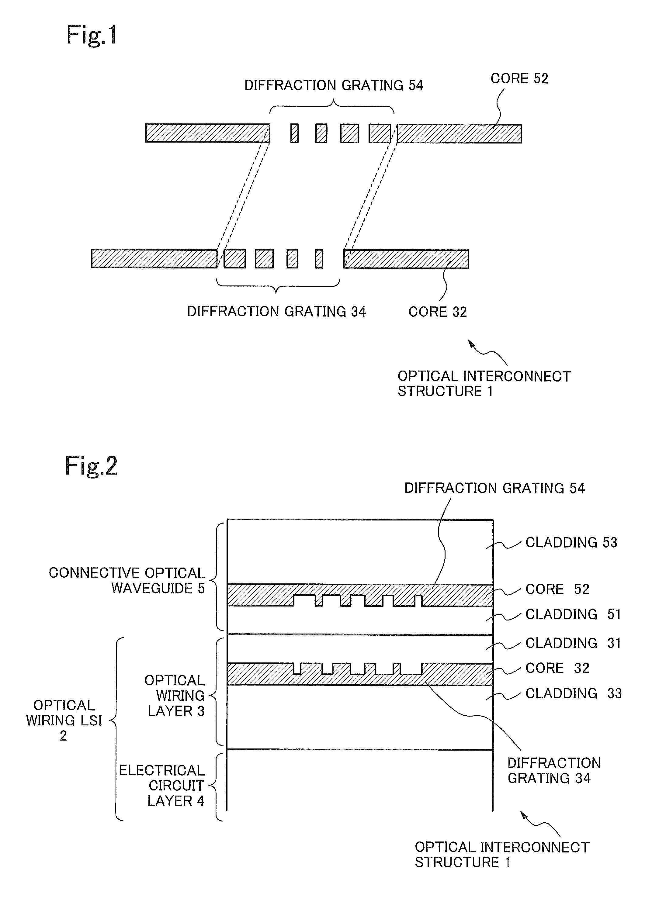
[0022]Next, a first exemplary embodiment will be described below. FIG. 1 shows a perspective view of only core layer portions extracted from an optical interconnect structure of the present exemplary embodiment. FIG. 2 shows a cross-sectional view of the optical interconnect structure 1.

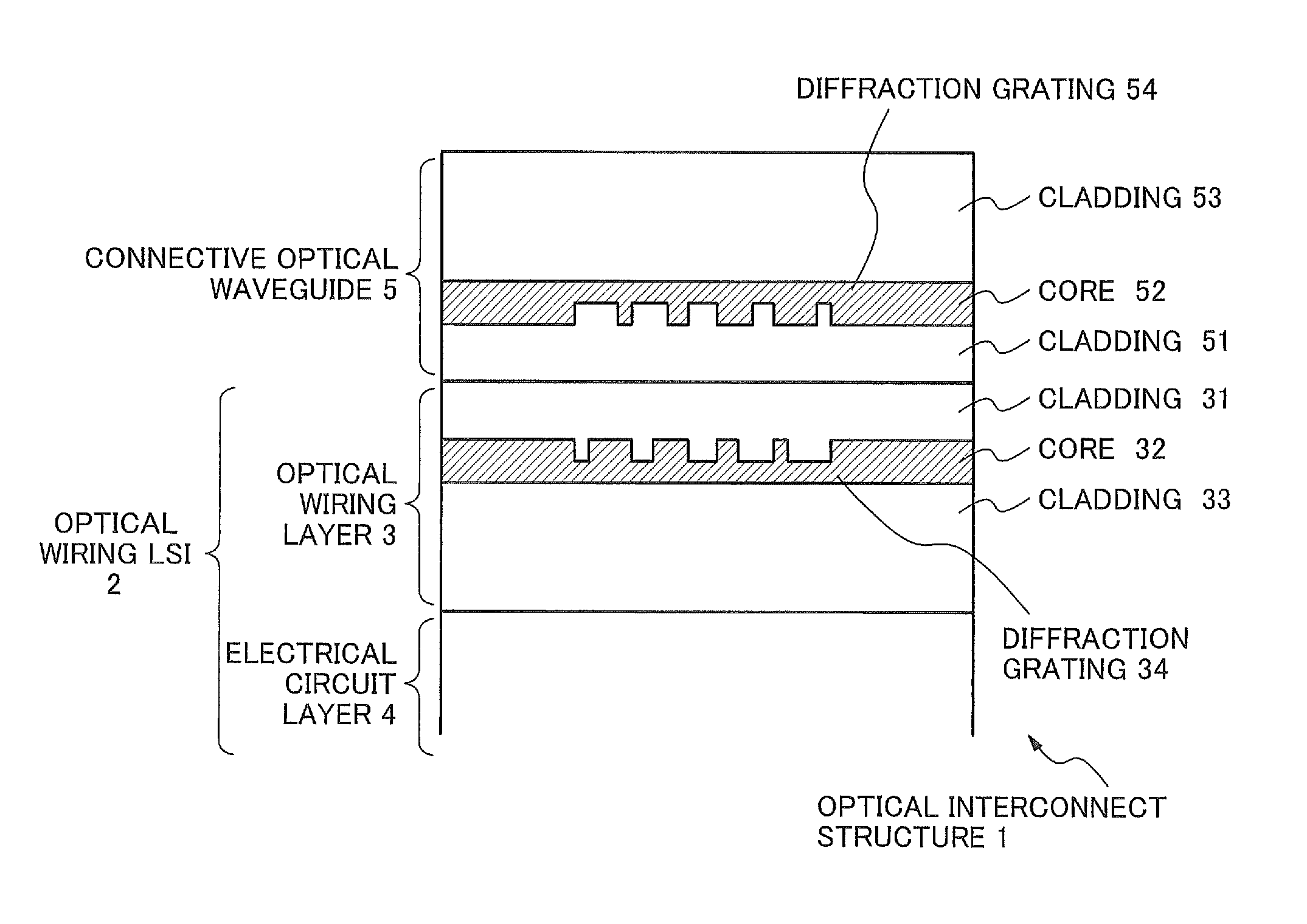
[0023]As shown in FIG. 2, the optical interconnect structure 1 of the present exemplary embodiment comprises an optical wiring LSI 2 comprising an optical wiring layer 3, and also comprises a connective optical waveguide 5.

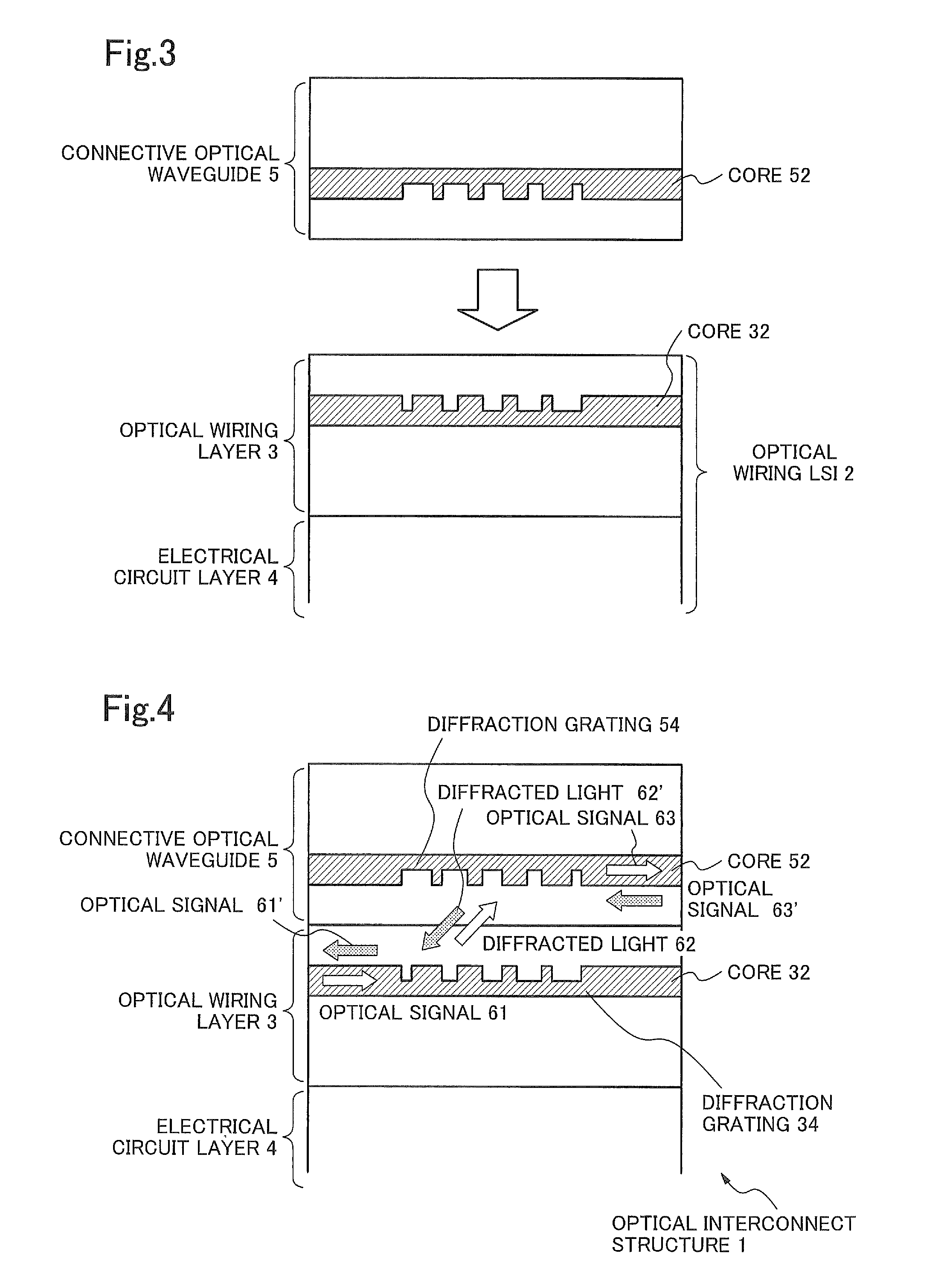
[0024]FIG. 3 is a transverse cross-sectional view showing a positional relationship between the optical wiring LSI 2 and the connective optical waveguide 5 before their connection. FIG. 4 is a transverse cross-sectional view showing a positional relationship between the optical wiring LSI 2 and the connective optical waveguide 5 after their connection.

[0025]In the optical interconnect structure 1, the detachable connective optical waveguide 5 is connected onto the optical wiring LS...

second exemplary embodiment

[0048]Next, a second exemplary embodiment will be described with reference to a drawing. FIG. 5 is a diagram showing the second exemplary embodiment, where a perspective view of only core layer portions extracted respectively from an optical wiring layer 3 and a connective optical waveguide 5 is illustrated.

[0049][Description of structure] In the present exemplary embodiment, similarly to in the first exemplary embodiment, an optical interconnect structure 1 comprises an optical wiring LSI 2 comprising an optical wiring layers 3, and also comprises a connective optical waveguide 5. The optical wiring layer 3 comprises a core 32 in which a diffraction grating 34 is formed, and the connective optical waveguide 5 comprises a core 52 in which a diffraction grating 54 is formed. Then, the diffraction gratings 34 and 54 are arranged such that at least a part of one of them faces a part of the other.

[0050]A difference of the present exemplary embodiment from the first exemplary embodiment ...

third exemplary embodiment

[0054]Next, a third exemplary embodiment will be described below.

[0055][Description of structure] In the present exemplary embodiment, similarly to in the second exemplary embodiment, an optical interconnect structure 1 comprises an optical wiring LSI 2 comprising an optical wiring layers 3, and also comprises a connective optical waveguide 5. The optical wiring layer 3 comprises a core 32 in which a diffraction grating 34 is formed, and the connective optical waveguide 5 comprises a core 52 in which a diffraction grating 54 is formed. Then, the diffraction gratings 34 and 54 are arranged such that at least a part of one of them faces a part of the other.

[0056]Further, in the present exemplary embodiment, the core 32 in the optical wiring layer 3 has a refractive index, Ncr3, equivalent to that of the core 52 in the connective optical waveguide 5, Ncr5, and claddings 31 and 33 in the optical wiring layer 3 have a refractive index, Ncl3, equivalent to that of claddings 51 and 53 in t...


PUM


Abstract

The present invention is an optical interconnect structure characterized by that it comprises an optical waveguide comprising a first core and a connective optical waveguide which is formed on the optical waveguide and comprises a second core, and that a first diffraction grating formed in the first core and a second diffraction grating formed into the second core are arranged such that at least a part of the former faces a part of the latter.

Description

TECHNICAL FIELD[0001]The present invention relates to an LSI with on-chip optical wirings, and in particular, to an optical interconnect structure for optical interconnection with an external light source and that between optical wiring LSI chips.BACKGROUND ART[0002]With the size reduction of transistors, integration density of semiconductor integrated circuits has been increased, and processing speed of electrical signals still continues increasing. Electrical signal wiring in semiconductor integrated circuits, particularly, global wiring, which is relatively long range wiring, has problems of wiring delay, degradation in signal quality (skew, jitter) and the like, and also problems of signal degradation due to crosstalk between electrical wirings adjacent to each other and of being susceptible to the noise from the surroundings of the semiconductor integrated circuit. The delay of global wiring has been suppressed by insertion of a repeater circuit. However, because of increase in...

Claims


Application Information

Patent Timeline
Patent Type & Authority Patents(United States)
IPC IPC(8): G02B6/34G02B6/12G02B6/124G02B6/122G02B6/293
CPCG02B6/34G02B6/12002G02B6/124G02B6/1228G02B6/29334
Inventor SHIMIZU, TAKANORI
Owner NEC CORP
Why Eureka
Try Eureka