Capacitive fingerprint sensor with improved sensing element

a fingerprint sensor and sensing element technology, applied in the field of capacitive fingerprint sensing devices, can solve the problems the fingerprint sensor with such a thin protective coating is not robust enough for many important applications, and the time-varying potential difference between the sensing structure and the semiconductor substrate, so as to reduce the influence of parasitic capacitance in the sensing elemen

Active Publication Date: 2015-10-06
FINGERPRINT CARDS ANACATUM IP AB
View PDF8 Cites 67 Cited by
  • Summary
  • Abstract
  • Description
  • Claims
  • Application Information

AI Technical Summary

Benefits of technology

[0053]In summary, the present invention relates to a capacitive fingerprint sensing device comprising a semiconductor substrate; and an array of sensing elements formed on the semiconductor substrate. Each of the sensing elements comprises a protective dielectric top layer; a sensing structure arranged underneath the top layer; and a charge amplifier connected to the sensing structure. The charge amplifier comprises a negative input connected to the sensing structure; a positive input; an output pro...

Problems solved by technology

This, however, requires a relatively large capacitance.
A fingerprint sensor with such a thin protective coating would not be robust enough for many important applications, including mobile device applications.
If, however, the excitation signal is applied to the sensing structure, there will be a time varying potential difference between the sensing structure...

Method used


Image

  • Capacitive fingerprint sensor with improved sensing element
  • Capacitive fingerprint sensor with improved sensing element
  • Capacitive fingerprint sensor with improved sensing element

Examples


Embodiment Construction

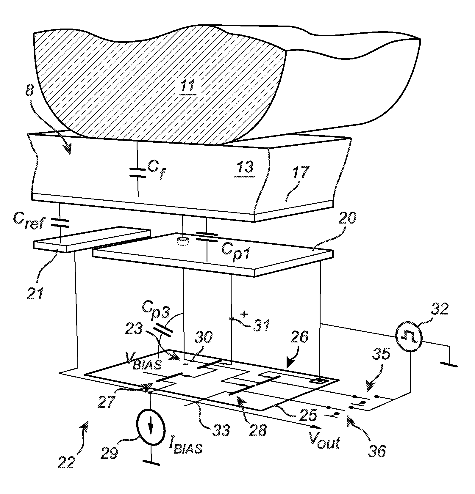
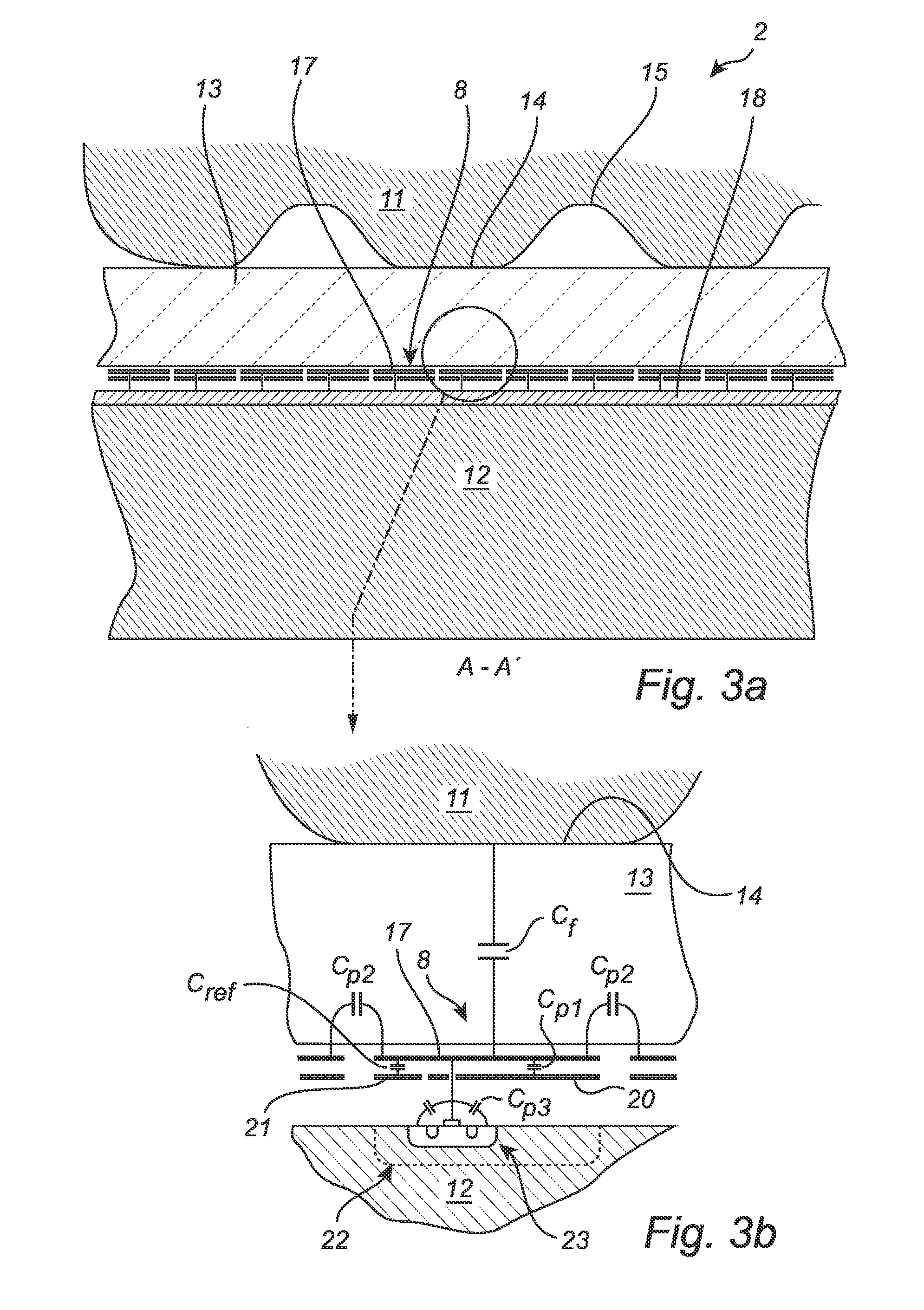
[0066]In the present detailed description, various embodiments of the fingerprint sensing device and method according to the present invention are mainly described with reference to a fingerprint sensing device in which positive input of the charge amplifier and the well in which the sense transistor comprised in the charge amplifier is formed are connected together and accordingly controlled by the excitation signal providing circuitry to follow the same time-varying electrical potential (in relation to a reference potential, such as electrical ground). The shielding plate between the sensing structure (plate) and the underlying structures in the fingerprint sensing device is also connected to the positive input of the charge amplifier. Furthermore, the feedback capacitor is formed by the sensing plate, a reference plate in the same metal layer as the above-mentioned shielding plate and the dielectric layer between the sensing plate and the reference plate. Moreover, the fingerprin...


PUM


Abstract

The present invention relates to a capacitive fingerprint sensing device comprising a semiconductor substrate; and an array of sensing elements formed on the semiconductor substrate. Each of the sensing elements comprises a protective dielectric top layer; a sensing structure arranged underneath the top layer; and a charge amplifier connected to the sensing structure. The charge amplifier comprises a negative input connected to the sensing structure; a positive input; an output providing a sensing signal; a feedback capacitor; and a sense transistor having a gate constituting the negative input. The sense transistor is formed in an insulated well in the semiconductor substrate. The fingerprint sensing device further comprises excitation signal providing circuitry connected to the positive input of the charge amplifier and the well for changing electric potentials of the sensing structure and the well, to thereby reduce the influence of parasitic capacitances in the sensing element.

Description

FIELD OF THE INVENTION[0001]The present invention relates to a capacitive fingerprint sensing device and to a method of sensing a fingerprint pattern.BACKGROUND OF THE INVENTION[0002]Various types of biometric systems are used more and more in order to provide for increased security and / or enhanced user convenience.[0003]In particular, fingerprint sensing systems have been adopted in, for example, consumer electronic devices, thanks to their small form factor, high performance and user acceptance.[0004]Among the various available fingerprint sensing principles (such as capacitive, optical, thermal etc), capacitive sensing is most commonly used, in particular in applications where size and power consumption are important issues.[0005]All capacitive fingerprint sensors provide a measure indicative of the capacitance between each of several sensing structures and a finger placed on or moved across the surface of the fingerprint sensor.[0006]Some capacitive fingerprint sensors passively...

Claims


Application Information

Patent Timeline
IPC IPC(8): G06K9/00G07C9/00G06K9/03G06V10/98G06V40/13
CPCG06K9/0002G06K9/0008G07C9/00158G06K9/036A61B5/1172A61B2562/046A61B2562/0214G07C9/37G06V40/1306G01R27/26G06V40/1329G01R27/2605G06V40/1359G06V10/993
Inventor RIEDIJK, FRANK ROBERT
Owner FINGERPRINT CARDS ANACATUM IP AB
Why Eureka
Try Eureka