
Optical semiconductor device and optical pickup device

a pickup device and optical semiconductor technology, applied in the direction of radio frequency controlled devices, instruments, record information storage, etc., can solve the problems of parasitic capacitance of the wiring and frequency characteristic deterioration, and achieve the effect of preventing the deterioration of the frequency characteristic of the optical pickup device, and reducing the influence of parasitic capacitan

Inactive Publication Date: 2008-03-06
PANASONIC CORP
View PDF8 Cites 7 Cited by
  • Summary
  • Abstract
  • Description
  • Claims
  • Application Information

AI Technical Summary

Benefits of technology

[0011]Consequently, an object of the present invention is to provide an optical semiconductor device which reduces an influence of a parasitic capacitance and also prevents a deterioration of a frequency characteristic.
[0029]The present invention can provide the optical semiconductor device which reduces the influence of the parasitic capacitance and also prevents the deterioration of the frequency characteristic.FURTHER INFORMATION ABOUT TECHNICAL BACKGROUND TO THIS APPLICATION

Problems solved by technology

However, the conventional optical semiconductor device described above has the following problem.
The output stage has a large current capacity and a low transfer impedance, so that the parasitic capacitance of the wiring has a low influence on the output stage, however, the wiring in the amplifier, more particularly, the connection wire of a differential amplifier passes only a small amount of current and has apparently a high transfer impedance, so that when the voltage amplitude which is equal to the amplitude of the converted voltage signal is transmitted, the connection wire is susceptible to the parasitic capacitance of the wiring, and deterioration in the frequency characteristic occurs.

Method used


Image

  • Optical semiconductor device and optical pickup device
  • Optical semiconductor device and optical pickup device
  • Optical semiconductor device and optical pickup device

Examples


first embodiment

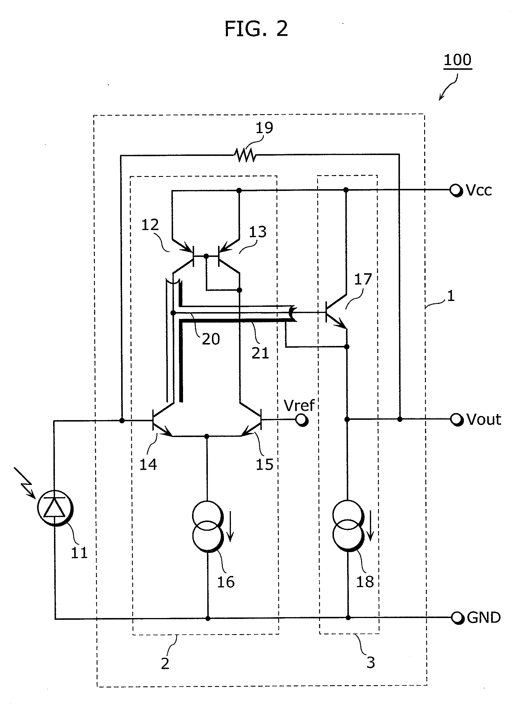
[0043]An optical semiconductor device according to the first embodiment of the present invention shields a connection wire of a differential amplifier which makes up a current-voltage conversion amplifier, with a shield wire which is connected to an output of the current-voltage conversion amplifier. According to this configuration, the parasitic capacitance for the connection wire in the differential amplifier can be reduced, and the deterioration of the frequency characteristic can be prevented.

[0044]First, a configuration of the optical semiconductor device according to the first embodiment of the present invention is described.

[0045]FIG. 2 is a circuit diagram showing the configuration of the optical semiconductor device according to the first embodiment of the present invention.

[0046]An optical semiconductor device 100 shown in FIG. 2 includes a light-receiving element 11 and a current-voltage conversion amplifier 1. The light-receiving element 11 converts a radiated light sign...

second embodiment

[0070]In the second embodiment of the present invention, an optical semiconductor device whose amplifier configuration in a voltage-current conversion amplifier is changed from the configuration of the first embodiment is described.

[0071]First, a configuration of the optical semiconductor device according to the second embodiment of the present invention is described.

[0072]FIG. 9 is a circuit diagram showing the configuration of the optical semiconductor device according to the second embodiment of the present invention. An optical semiconductor device 200 shown in FIG. 9 includes a light-receiving element 11 and a current-voltage conversion amplifier 201. In the optical semiconductor device 200, a configuration of an amplifier 202 in the current-voltage conversion amplifier 201 is different from that of the optical semiconductor device 100 shown in FIG. 2.

[0073]The light-receiving element 11 converts the light signal, with which the light-receiving element 11 is irradiated, into a ...

third embodiment

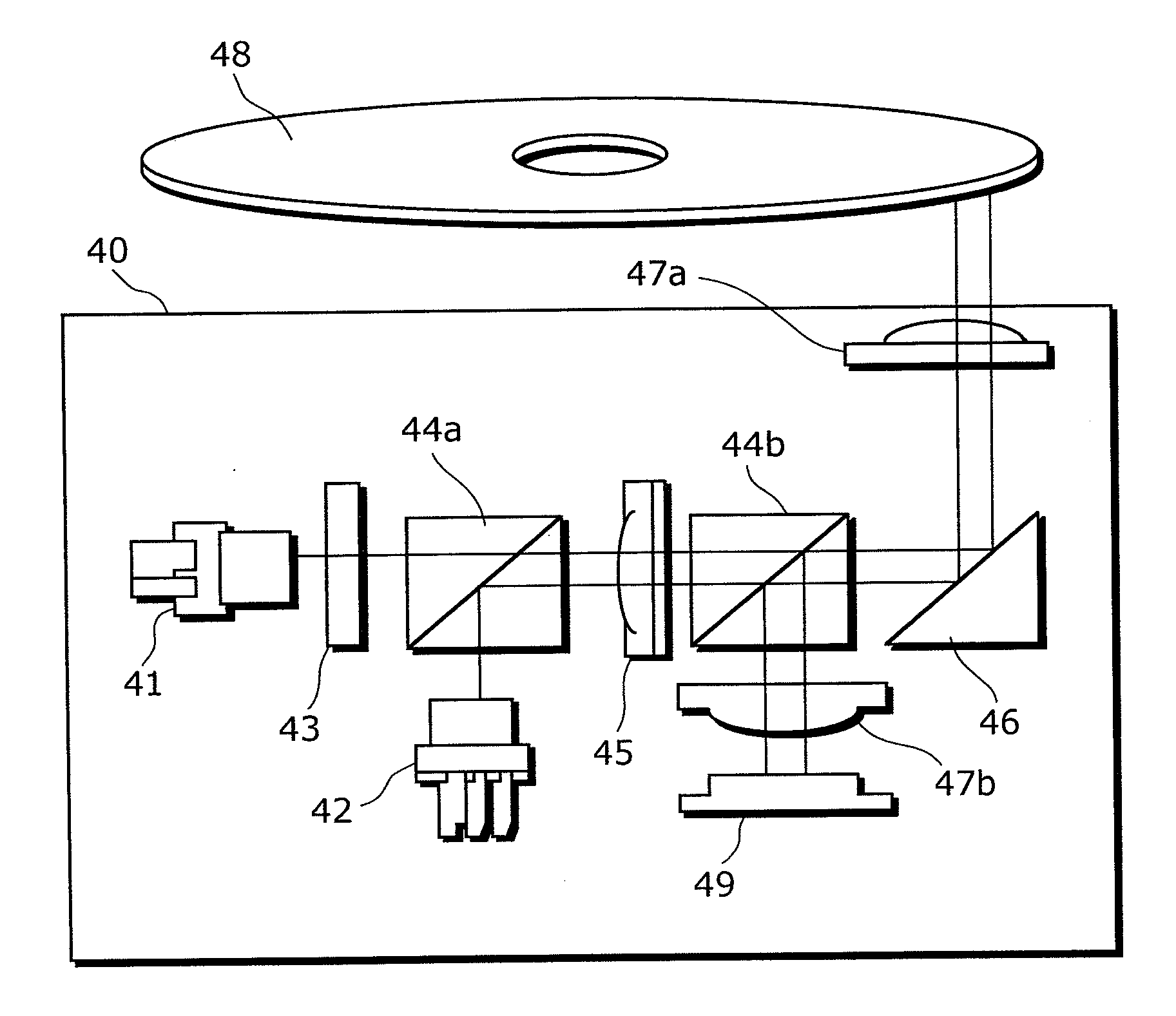
[0087]In the third embodiment of the present invention, an example that the optical semiconductor device described above is applied to an optical pickup device is described.

[0088]FIG. 10 shows a configuration of the optical pickup device according to the third embodiment of the present invention.

[0089]An optical pickup device 40 shown in FIG. 10 accepts both DVD and CD. The optical pickup device 40 reads out data from an optical disk medium 48 and writes data to the optical disk medium 48. The optical pickup device 40 includes an infrared laser 41, a red laser 42, a three-beam grating 43, beam splitters 44a and 44b, a collimator lens 45, a mirror 46, objective lens 47a and 47b, and a light-receiving IC 49. The light-receiving IC 49 receives a laser light which is reflected by the optical disk medium 48. The light-receiving IC 49 includes the various optical semiconductor devices 100 according to the first embodiment shown in FIG. 2, for example.

[0090]First, an operation in accepting...


PUM

PropertyMeasurementUnit
angleaaaaaaaaaa
currentaaaaaaaaaa
voltageaaaaaaaaaa

Abstract

An optical semiconductor device of the present invention includes: a light-receiving element which converts light into an electric signal; an amplifier circuit having an input terminal to which the light-receiving element is connected, and which amplifies the electric signal; a connection wire to which the signal amplified by the amplifier circuit is outputted; an output circuit having an input terminal to which the connection wire is connected, and which performs current amplification on the signal amplified by the amplifier circuit and outputs the current-amplified signal to an output terminal; a feedback resistor connected between the input of the amplifier circuit and the output terminal; and a shield wire connected to a potential outputted from the output circuit or a potential resulting from a voltage follower of the potential outputted from the output circuit, and which shields the connection wire from noise.

Description

BACKGROUND OF THE INVENTION[0001](1) Field of the Invention[0002]The present invention relates to an optical semiconductor device and an optical pickup device, and more particularly, to an optical semiconductor device which converts light into an electric signal and outputs the electric signal.[0003](2) Description of the Related Art[0004]In recent years, the increase in the size of circuits is progressing with the increase in integration, function and speed of semiconductor integrated circuit devices. Accordingly, wirings become longer, and frequency characteristic deterioration due to the parasitic capacitance of the wirings is becoming a problem.[0005]An optical pickup device includes a laser generator which irradiates an optical disk medium with a laser light used for each of a CD (Compact Disk) and a DVD (Digital Versatile Disc), and an optical semiconductor device which receives and amplifies the reflected light. The optical semiconductor device includes plural light-receiving...

Claims


Application Information

Patent Timeline
Patent Type & Authority Applications(United States)
IPC IPC(8): G11B7/00H03F3/08H01L31/00
CPCG11B7/13H01L27/144H03F3/08H03F3/087H03F3/45085H03F2203/45722H03F2203/45138H03F2203/45166H03F2203/45224H03F2203/45266H03F3/45475
Inventor FUKUDA, HIDEOMIYAMOTO, SHINICHI
Owner PANASONIC CORP
Learn More