Organic electroluminescent device

an electroluminescent device and organ technology, applied in the field of organic electroluminescence devices, can solve problems such as efficiency improvement, and achieve the effect of high efficiency and efficient inducing the ttf phenomenon

Active Publication Date: 2015-10-06
IDEMITSU KOSAN CO LTD
View PDF87 Cites 25 Cited by
  • Summary
  • Abstract
  • Description
  • Claims
  • Application Information

AI Technical Summary

Benefits of technology

[0220]The advantageous effects brought by the blocking layer are significant comparing to the luminous efficiency conventionally attained in a blue fluorescent device. In a green fluorescent device and a red fluorescent device, similar advantageous effects, i.e. effects of confining triplet energies in the emitting layer, can be attained, and improvement in luminous efficiency can also be expected.
[0221]On the other hand, in a phosphorescent emitting layer, it is possible to attain the advantageous effects of confining triplet energies in the emitting layer, and as a result, diffusion of triplet energies is prevented, thereby contributing to improvement in luminous efficiency of a phosphorescent dopant.
[0222]The hole-transporting region is formed of a hole-transporting layer, or a combination of a hole-transporting layer and a hole-injecting layer, or the like. A common hole-transporting region may be provided or different hole-transporting regions may be provided. Normally, the hole-transporting regions respectively have a configuration suited to the color of emitted light.
[0223]The configuration of the organic layer formed of an emitting layer 20B, an emitting layer 20G, an emitting layer 20R and the blocking layer is not limited to that shown in the figure, and it can be changed appropriately.
[0224]The host and dopant that can be used in the present invention are described above. In particular, each color emitting layer will be described hereinbelow.
[0225]A green color emitting layer is preferably formed of the following host materials and dopant materials. The host materials are preferably condensed aromatic ring derivatives. As the condensed aromatic ring derivatives, anthracene derivatives, pyrene derivatives or the like are more preferable in view of luminous efficiency or lifetime.

Problems solved by technology

In a phosphorescent device, efficient confinement of triplet excitons within an emitting layer does not necessarily result in improvement in efficiency.

Method used


Image

  • Organic electroluminescent device
  • Organic electroluminescent device
  • Organic electroluminescent device

Examples


first embodiment

[0049]The invention utilizes the TTF phenomenon. First, an explanation is made of the TTF phenomenon.

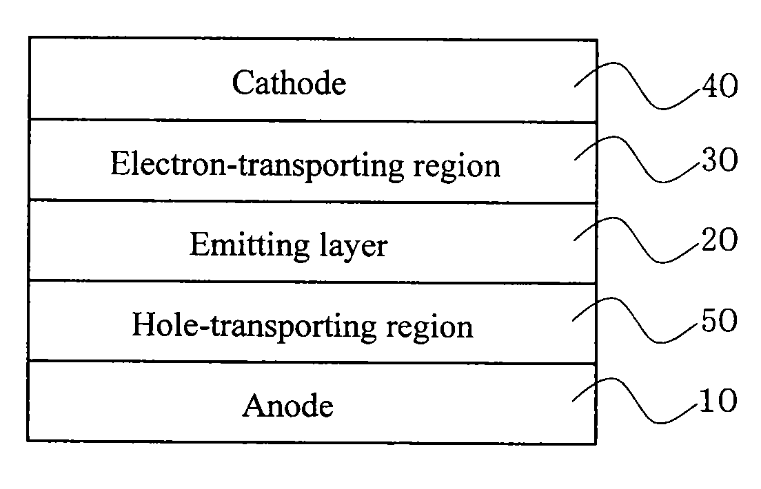
[0050]Holes and electrons injected from an anode and a cathode are recombined with an emitting layer to generate excitons. As for the spin state, as is conventionally known, singlet excitons account for 25% and triplet excitons account for 75%. In a conventionally known fluorescent device, light is emitted when singlet excitons of 25% are relaxed to the ground state. The remaining triplet excitons of 75% are returned to the ground state without emitting light through a thermal deactivation process. Accordingly, the theoretical limit value of the internal quantum efficiency of a conventional fluorescent device is believed to be 25%.

[0051]The behavior of triplet excitons generated within an organic substance has been theoretically examined. According to S. M. Bachilo et al. (J. Phys. Chem. A, 104, 7711 (2000)), assuming that high-order excitons such as quintet excitons are quickly retu...

second embodiment

[0192]The device of the invention may have a tandem device configuration in which at least two organic layer units including emitting layers are provided. An intermediate layer (intermediate conductive layer, charge generation layer or CGL) is provided between the two emitting layers. An electron-transporting region can be provided in each unit. At least one emitting layer is a fluorescent emitting layer and the unit including the emitting layer satisfies the above-mentioned requirements. Specific examples of stack order are given below. The following emitting layer may be a multilayer stack of emitting layers or one organic layer unit including a carrier blocking layer of a third embodiment described later.

[0193]Anode / fluorescent emitting layer / intermediate layer / fluorescent emitting layer / blocking layer / cathode

[0194]Anode / fluorescent emitting layer / blocking layer / intermediate layer / fluorescent emitting layer / cathode

[0195]Anode / fluorescent emitting layer / blocking layer / intermediate...

third embodiment

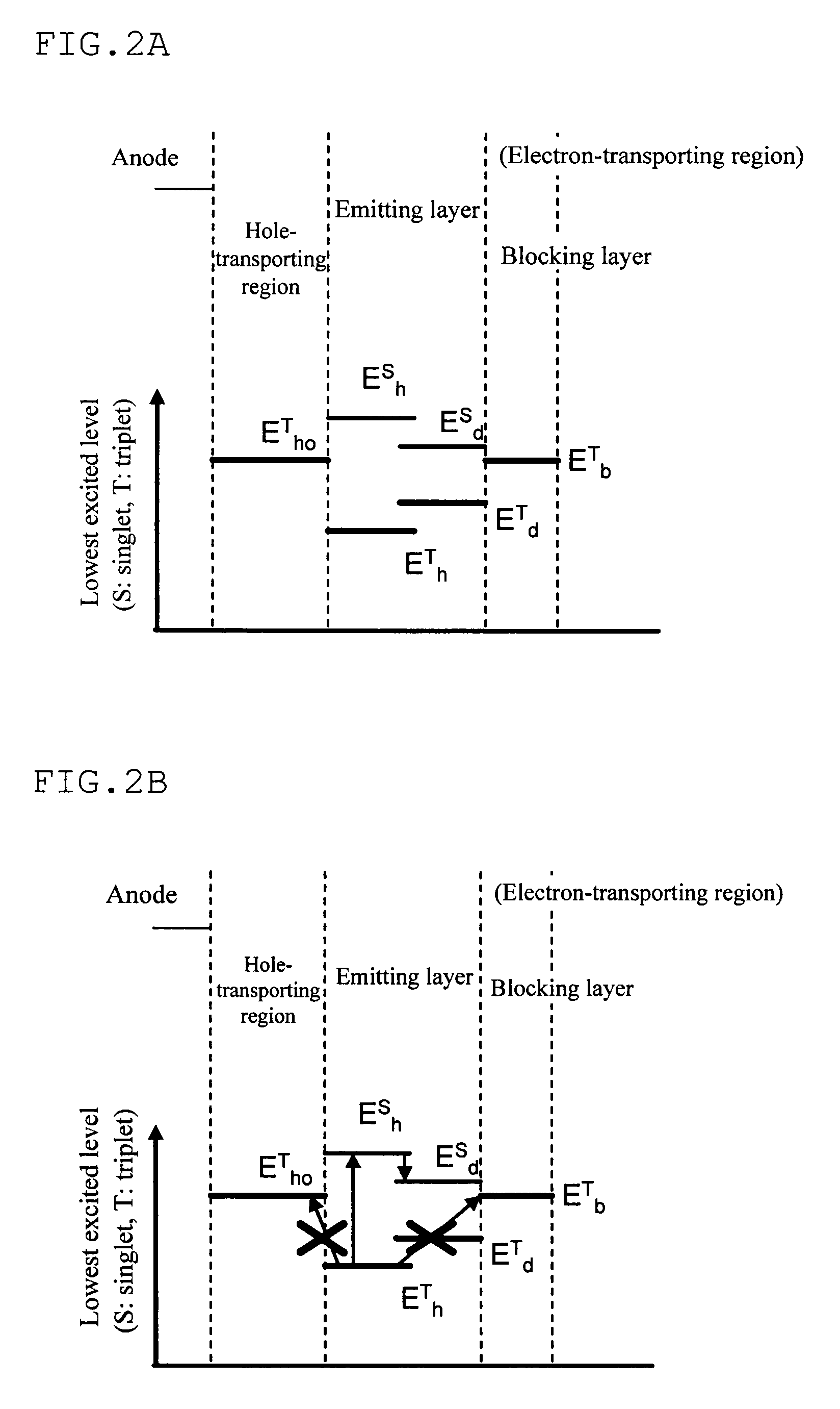
[0202]In this embodiment, an anode, a plurality of emitting layers, an electron-transporting region, and a cathode are provided in sequential order, and a carrier blocking layer is provided between two of the emitting layers. The emitting layer in contact with the carrier blocking layer is a fluorescent emitting layer satisfying the above-mentioned requirements.

[0203]As the preferred configuration of the organic EL device according to this embodiment, there can be given the configuration as disclosed in Japanese Patent No. 4134280, US2007 / 0273270A1 and WO2008 / 023623A1, and, specifically, the configuration in which an anode, a first emitting layer, a carrier blocking layer, a second emitting layer and a cathode are sequentially stacked, and an electron-transporting region having a blocking layer for preventing diffusion of triplet excitons is further provided between the second emitting layer and the cathode. Here, the carrier blocking layer means a layer to control the carrier injec...


PUM

PropertyMeasurementUnit
peak wavelengthaaaaaaaaaa
current efficiencyaaaaaaaaaa
electric field intensityaaaaaaaaaa

Abstract

An organic electroluminescence device including an anode, an emitting layer, a blocking layer, an electron-injecting layer and a cathode in sequential order; wherein the emitting layer contains a host and a dopant which gives fluorescent emission of which the main peak wavelength is 550 nm or less; the affinity Ad of the dopant is smaller than the affinity Ah of the host; the triplet energy ETd of the dopant is larger than the triplet energy ETh of the host; the triplet energy ETb of the blocking layer is larger than ETh; and the blocking layer includes an aromatic hydrocarbon compound.

Description

CROSS-REFERENCE TO RELATED APPLICATIONS[0001]This application is a continuation-in-part of U.S. Ser. No. 12 / 478,290 filed May 4, 2009, abandoned, and claims the benefit of JP 2009-124760 filed May 22, 2009 and JP 2009-125883 filed May 25, 2009.TECHNICAL FIELD[0002]The invention relates to an organic electroluminescence (EL) device, particularly, to a highly efficient organic EL device.BACKGROUND ART[0003]An organic EL device can be classified into two types, i.e. a fluorescent EL device and a phosphorescent EL device according to its emission principle. When a voltage is applied to an organic EL device, holes are injected from an anode, and electrons are injected from a cathode, and holes and electrons recombine in an emitting layer to form excitons. According to the electron spin statistics theory, singlet excitons and triplet excitons are formed at an amount ratio of 25%:75%. In a fluorescent EL device which uses emission caused by singlet excitons, the limited value of the intern...

Claims


Application Information

Patent Timeline
Patent Type & Authority Patents(United States)
IPC IPC(8): H01L51/50C09B1/00C09B57/00H01L51/00
CPCH01L51/5016C09B1/00C09B57/00C09B57/001C09B57/008H01L51/5096H01L51/0052H01L51/0059H01L51/0072H01L51/0073H10K85/615H10K85/631H10K85/6574H10K85/6572H10K50/18H10K50/11H10K2101/10
Inventor KUMA, HITOSHIKAWAMURA, YUICHIROJINDE, YUKITOSHIOGIWARA, TOSHINARIHOSOKAWA, CHISHIO
Owner IDEMITSU KOSAN CO LTD
Why Eureka
Try Eureka