Semiconductor laser diode device and method of fabrication thereof

a laser diode and semiconductor technology, applied in semiconductor lasers, laser details, optical resonator shape and construction, etc., can solve the problems of difficult to provide different grating depths, produce sufficient degree of difference, and difficult control processes, so as to reduce the degree of wavelength chirping, reduce the transmission limit distance, and ensure the stability of single-mode oscillation.

Active Publication Date: 2013-07-02
RENESAS ELECTRONICS CORP
View PDF15 Cites 25 Cited by
  • Summary
  • Abstract
  • Description
  • Claims
  • Application Information

AI Technical Summary

Benefits of technology

[0010]In contrast, significantly advantageous effects can be attained by providing different optical coupling coefficient values κ in different regions of an optical waveguide.
[0011]For example, if a configuration having a relatively large value of optical coupling coefficient κ only in a device rear region of an optical waveguide is formed and applied to AR / AR DFB-LD design, it becomes possible to produce an AR / AR DFB-LD device capable of providing a forward / backward optical output ratio as high as that of an AR / HR DFB-LD device while ensuring satisfactory stability of single-mode oscillation that is characteristic of AR / AR DFB-LD design. In Patent Document 3 indicated below, there is disclosed an AR / HR DFB-LD configuration in which a relatively large value of optical coupling coefficient κ is provided in a device rear region by using a different etched grating pattern (depth) therein. Patent Document 4 indicated below discloses a configuration in which a value of optical coupling coefficient κ varies gradually from a device front position to a device rear position (different heights of grating are provided), along with the description of a method of fabrication thereof. Patent Document 5 indicated below discloses a configuration in which a guide layer is provided with a buried grating structure, a partial composition of a rear region of the guide layer being arranged to be different from the composition of a front region of the guide layer (the rear region has a composition for a wavelength longer than that in the front region), and the depth of a grating structure part buried with the guide layer in the front region being arranged to be different from that in the rear region. The disclosure of a method for fabricating the above configuration is also included in the Patent Document 5.
[0012]Further, as another example for attaining advantageous effects by providing different optical coupling coefficient values κ in different optical waveguide regions, it has been proposed to form a configuration in which a value of optical coupling coefficient κ in the vicinity of a λ / 4 phase shift part is smaller than that in the other regions.
[0013]Generally, at the time of laser oscillation in a DFB-LD device, the level of optical density becomes higher in the vicinity of a λ / 4 phase shift part. This is one of the causes of occurrence of wavelength chirping in modulation drive. The phenomenon “wavelength chirping” is an undesirable condition of wavelength variations on the order of Δv to several GHz, which brings about an adverse effect on optical signal communication such as a decrease in transmission limit distance. Hence, it is desirable to reduce the degree of wavelength chirping wherever possible.
[0014]It is already well known that the concentration of optical density in the vicinity of a λ / 4 phase shift part can be alleviated by providing a smaller value of optical coupling coefficient κ in the vicinity of λ / 4 phase shift part than that in the other regions. Thus, the degree of wavelength chirping can be reduced advantageously. For example, in Patent Document 6, there is disclosed a technique wherein the degree of wavelength variations in pulse modulation can be minimized without impairing the stability of single-longitudinal-mode oscillation under the conditions that the value of reflectivity at each of both front and rear facets is relatively small “=0.3%”, the value of κL (L: resonator length) is in a range of “0.8<κL<3.0” except a position in the vicinity of 1.3, and the value of phase shift Δθ in a discontinuous phase part at the center area of a resonator is in a range of “nπ+0.5π<Δθ<nπ+0.75π (λ / 4<Δθ<3λ / 8)”.
[0015]In Patent Document 9 indicated below, there is disclosed a DFB-LD device wherein a plurality of grating parts having mutually different pitches are disposed along the axial direction of an active layer.

Problems solved by technology

However, for the formation of this configuration, difficult-to-control processes are employed, e.g., an etching process for grating formation is performed on the basis of the dependency of an etching rate on the area of a photoresist pattern.
Further, it is rather difficult to provide different grating depths as intended to produce a sufficient degree of difference in terms of optical coupling coefficient κ. For example, in implementation of an AR / AR DFB-LD design arrangement wherein a relatively high value of optical coupling coefficient κ is provided in a device rear region of an optical waveguide for increasing a forward / backward optical output ratio, it is required to produce a degree of difference of approximately three times in grating depth between the device front and rear regions concerned.
This requirement is considerably difficult to meet in practical fabrication processing.

Method used


Image

  • Semiconductor laser diode device and method of fabrication thereof
  • Semiconductor laser diode device and method of fabrication thereof
  • Semiconductor laser diode device and method of fabrication thereof

Examples


first preferred embodiment

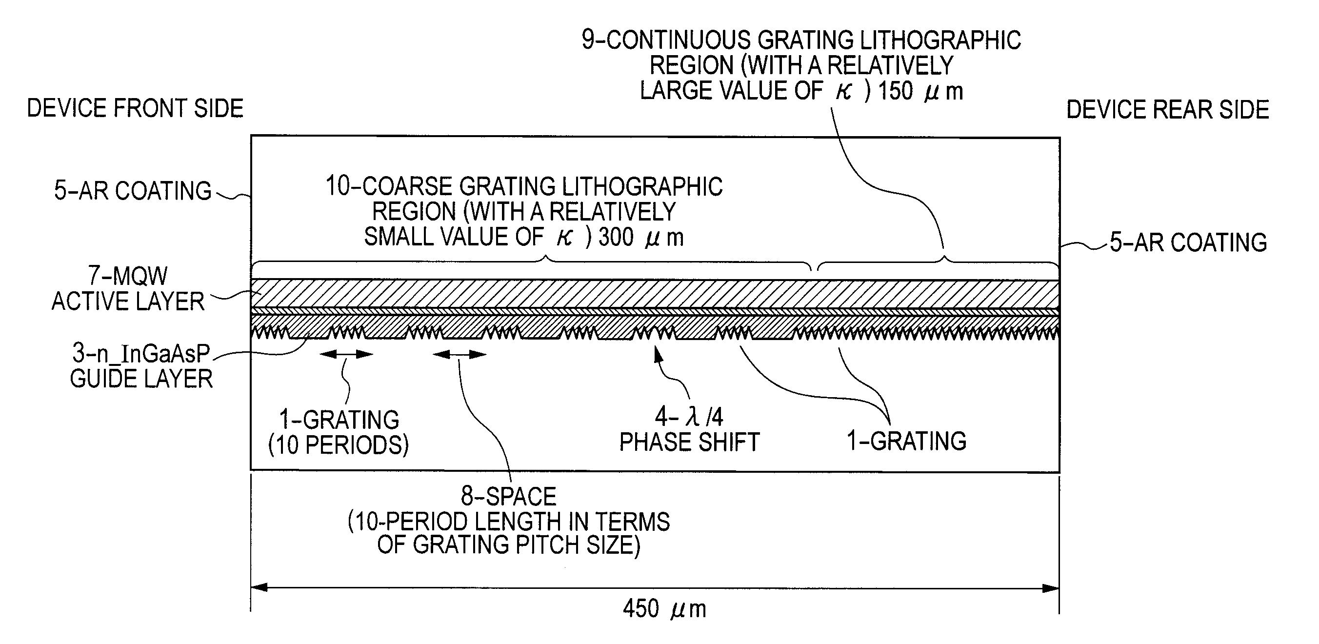
[0059]Referring to FIG. 1, there is shown a configuration of a DFB-LD device according to a first preferred embodiment of the present invention. In FIG. 1, a longitudinal cross-section parallel to the optical waveguide axial direction of the DFB-LD device is illustrated schematically. In a device front region of an optical waveguide according to the first preferred embodiment of the present invention, a grating 1 is formed to have ten periods, followed by a no-grating space part having a length of ten-period space, and an alternately repetitive pattern of the grating 1 and no-grating space part is provided (coarse grating lithographic region 10). The no-grating space part, which is indicated as “Space” with reference numeral 8 in FIG. 1, has a uniform refractive index. As a device rear region, there is provided a continuous grating lithographic region 9 of an ordinary type (continuous grating periodic region without partial missing of grating lines).

[0060]The average density of coar...

second preferred embodiment

[0099]Then, the following describes a second preferred embodiment of the present invention. Referring to FIG. 6, there is shown a configuration of a DFB-LD device according to the second preferred embodiment of the present invention. In FIG. 6, a longitudinal cross-section parallel to the optical waveguide axial direction of the DFB-LD device is illustrated schematically. According to the second preferred embodiment of the present invention, the device length L is 450 μm as in the case of the first preferred embodiment mentioned above, and a λ / 4 phase shift part 4 is disposed at a position of 300 λm from the device front end.

[0100]In the second preferred embodiment of the present invention, a coarse grating lithographic region 10 is provided in a length of 350 λm across the λ / 4 phase shift part 4 on the device front side. Further, in the coarse grating lithographic region 10 in the second preferred embodiment, there is formed an alternately repetitive pattern of a grating 1 having f...

third preferred embodiment

[0105]Then, the following describes a third preferred embodiment of the present invention. Referring to FIG. 7, there is shown a configuration of a DFB-LD device according to the third preferred embodiment of the present invention. In FIG. 7, a longitudinal cross-section parallel to the optical waveguide axial direction of the DFB-LD device is illustrated schematically. In the third preferred embodiment, as shown in FIG. 7, a λ / 4 phase shift part is not employed, differently from the case of the first preferred embodiment illustrated in FIG. 1. The other configurational features of the third preferred embodiment are the same as those of the first preferred embodiment in FIG. 1.

[0106]In the third preferred embodiment, a coarse grating lithographic region 10 is provided with an alternately repetitive pattern of a grating 1 having ten periods and a no-grating space part 8 (having a length of ten-period space). Note that, in the length of the space part 8, a factor of correction is incl...


PUM


Abstract

Disclosed is a distributed feedback semiconductor laser diode device capable of operating at a high output ratio of forward / backward optical power while ensuring satisfactory stability of single-mode oscillation. The distributed feedback semiconductor laser diode device is configured to include a diffraction grating formed in an optical waveguide thereof. In a partial region of the optical waveguide, there is formed an alternately repetitive pattern of a grating part possessing a distributive refractivity characteristic and a no-grating space part possessing a uniform refractivity characteristic. The no-grating space part possessing a uniform refractivity characteristic has an optical path length that is half an integral multiple of a wavelength of laser oscillation, and the grating part possessing a distributive refractivity characteristic includes at least five grating periods.

Description

CROSS-REFERENCE TO RELATED APPLICATIONS[0001]The disclosure of Japanese Patent Application No. 2009-275260 filed on Dec. 3, 2009 including the specification, drawings and abstract is incorporated herein by reference in its entirety.BACKGROUND OF THE INVENTION[0002]The present invention relates to semiconductor laser diode devices, and more particularly to a semiconductor laser diode device suitable for use as a light source in optical fiber communication and a method of fabrication thereof.[0003]There are two structural types of distributed feedback semiconductor laser diode (DFB-LD) devices; anti-reflection / anti-reflection (AR / AR) coated type, and anti-reflection / high-reflection (AR / HR) coated type. An AR / AR DFB-LD device is configured to have both front and rear facets thereof coated for anti-reflection as shown in FIG. 10, and an AR / HR DFB-LD device is configured to have a front facet thereof coated for anti-reflection and a rear facet thereof coated for high reflection as shown ...

Claims


Application Information

Patent Timeline
Patent Type & Authority Patents(United States)
IPC IPC(8): H01S5/00
CPCB82Y20/00H01S5/1209H01S5/1225H01S5/028H01S5/1206H01S5/1231H01S5/124H01S5/2222H01S5/227H01S5/34306
Inventor KITAMURA, SHOTARO
Owner RENESAS ELECTRONICS CORP
Why Eureka
Try Eureka