

System-in-packages and methods for forming same
a technology of system-in-package and method, applied in the direction of semiconductor devices, semiconductor/solid-state device details, electrical apparatus, etc., can solve the problems of warpage of interposers, unduly expensive and time-consuming processing, etc., to achieve faster processing time, reduce the process for forming the sip, and reduce the cost
- Summary
- Abstract
- Description
- Claims
- Application Information
AI Technical Summary
Benefits of technology
Problems solved by technology
Method used
Image

Examples
Embodiment Construction
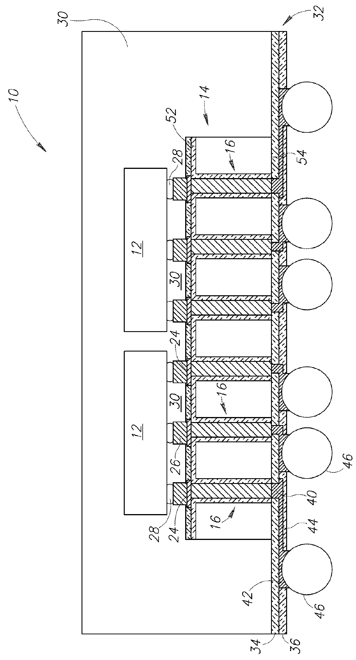
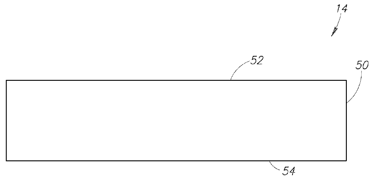
[0020]FIG. 1 illustrates a 2.5-D system-in-package (SiP) 10 in accordance with one embodiment of the present disclosure. The package 10 includes two or more semiconductor chips 12 having an electronic device, such as integrated circuits, formed on an active face thereof. The semiconductor chips 12 are mounted active face down and side by side in a flip chip configuration on a first side of an interposer 14. The interposer 14 may be any substrate configured to support the semiconductor chips 12. In some embodiments, the interposer 14 is silicon or glass.
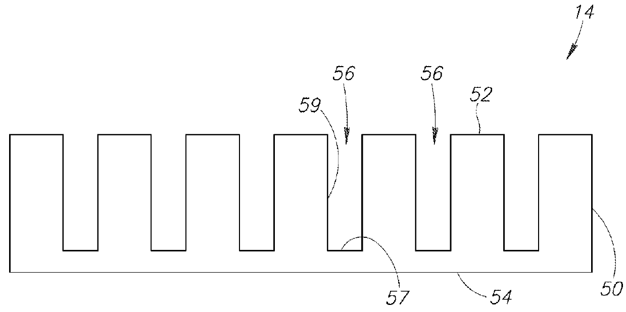
[0021]The interposer 14 includes conductive through vias 16 that extend from the first side 52 to a second side 54 of the interposer 14. Between the conductive through vias 16 at the first side 52 and the semiconductor chips 12 are metal interconnects 24, pillars 26, and solder bumps 28. The solder bumps 28 couple bond pads of the semiconductor chips 12 to the pillars 26.
[0022]An encapsulation layer 30 surrounds the semiconductor chip...
PUM
 Abstract
Description
Claims
Application Information