Eureka AIR delivers breakthrough ideas for toughest innovation challenges, trusted by R&D personnel around the world.

Imaging circuitry with robust scribe line structures

Active Publication Date: 2016-03-22
SEMICON COMPONENTS IND LLC
View PDF18 Cites 6 Cited by
  • Summary
  • Abstract
  • Description
  • Claims
  • Application Information

AI Technical Summary

Benefits of technology

The technical effect of this patent text is to provide better imaging systems for creating scribe lines.

Problems solved by technology

The lack of silicon substrate material in the scribe line regions may present challenges when forming color filter array structures for the image sensor die since the upper surface of the image sensor die tends to be non-uniform when at least a portion of the silicon substrate is removed in the scribe line regions.
The interface between the oxide material in the scribe line regions and adjacent silicon substrate material may be also be prone to damage and cracking during dicing operations.

Method used


Image

  • Imaging circuitry with robust scribe line structures
  • Imaging circuitry with robust scribe line structures
  • Imaging circuitry with robust scribe line structures

Examples


Embodiment Construction

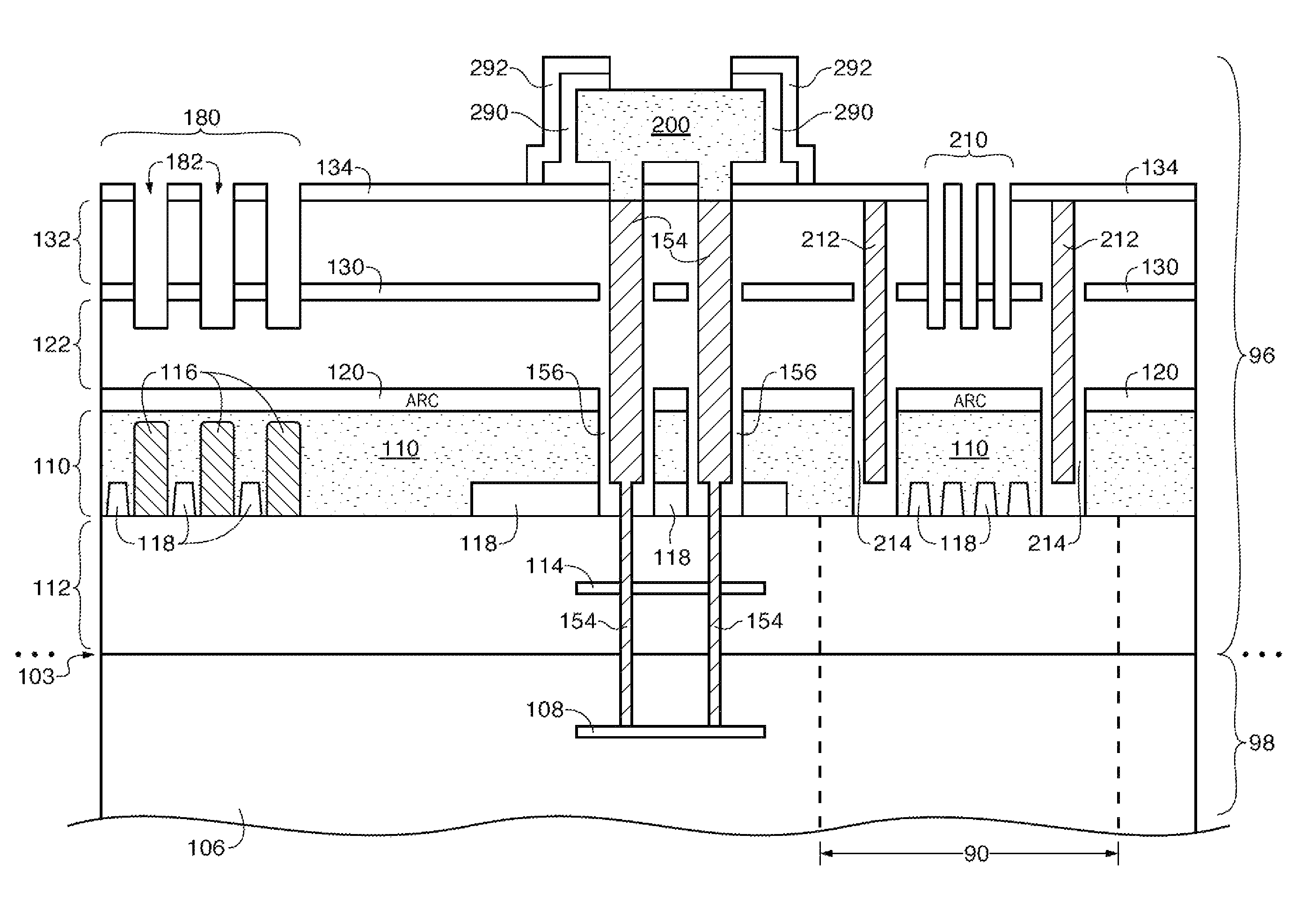
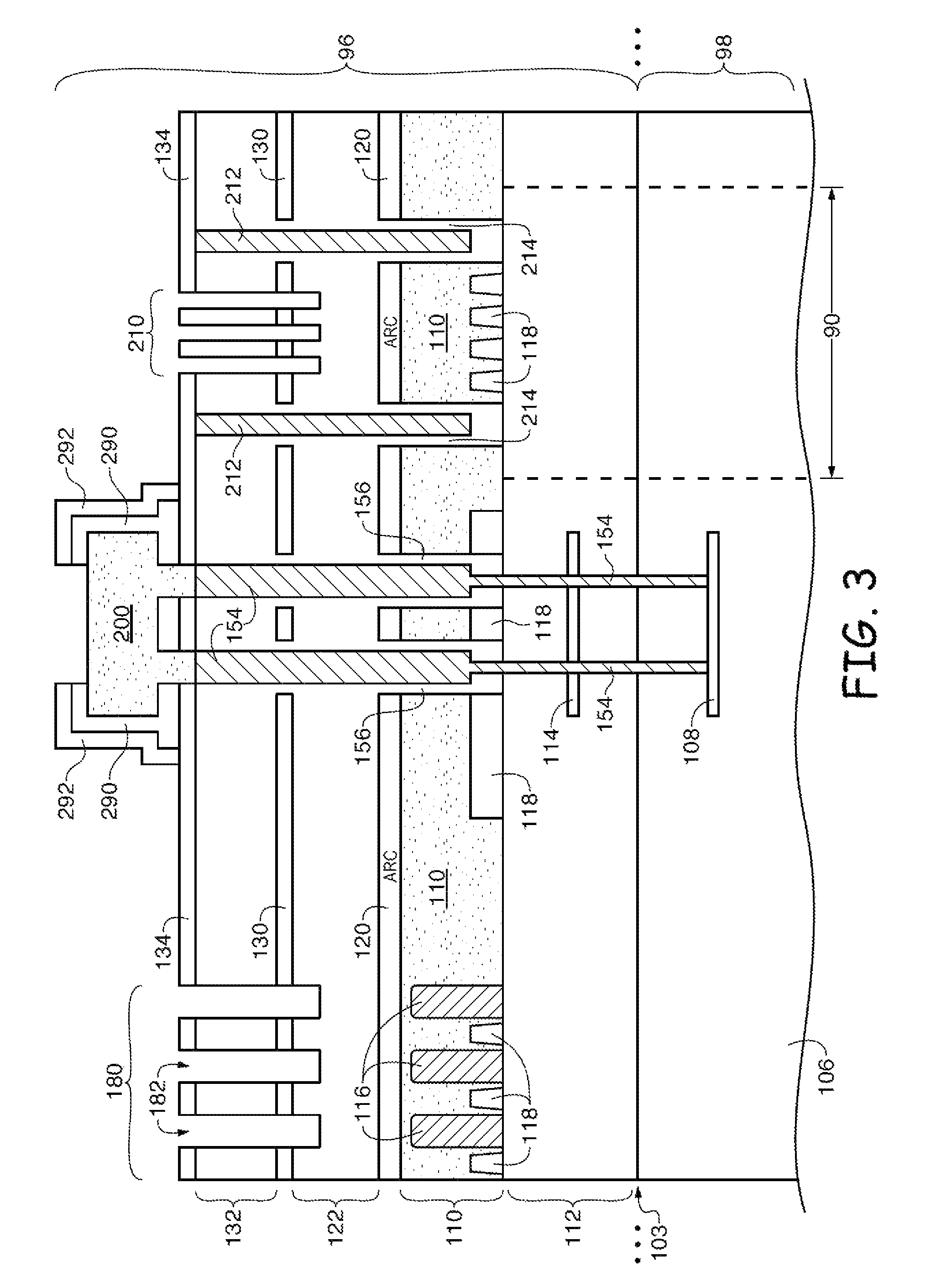
[0012]Electronic devices such as digital cameras, computers, cellular telephones, and other electronic devices include image sensors that gather incoming image light to capture an image. The image sensors may include arrays of imaging pixels. The pixels in the image sensors may include photosensitive elements such as photodiodes that convert the incoming image light into image signals. Image sensors may have any number of pixels (e.g., hundreds or thousands or more). A typical image sensor may, for example, have hundreds of thousands or millions of pixels (e.g., megapixels). Image sensors may include control circuitry such as circuitry for operating the imaging pixels and readout circuitry for reading out image signals corresponding to the electric charge generated by the photosensitive elements.

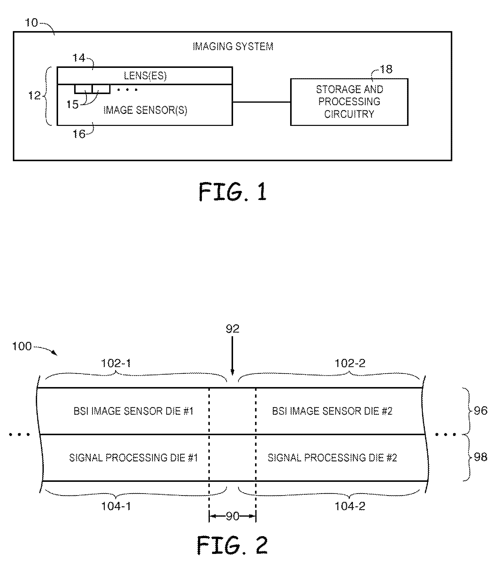
[0013]FIG. 1 is a diagram of an illustrative electronic device that uses an image sensor to capture images. Electronic device 10 of FIG. 1 may be a portable electronic device such as a camer...


PUM


Abstract

An image sensor wafer may be stacked on top of a digital signal processor (DSP) wafer. The image sensor wafer may include multiple image sensor dies, whereas the DSP wafer may include multiple DSP dies. The stacked wafers may be cut along scribe line regions to dice the wafers into individual components. Each image sensor die may include through-oxide vias (TOVs) that extend at least partially into a corresponding DSP die. Scribe line support structures may be formed surrounding the scribe line regions. The scribe line support structures and the TOVs may be formed during the same processing step. The TOVs can also be formed through deep trench isolation structures.

Description

BACKGROUND[0001]This relates generally to imaging systems, and more particularly, to imaging systems with stacked integrated circuit dies.[0002]Modern electronic devices such as cellular telephones, cameras, and computers often use digital image sensors. Imaging systems (i.e., image sensors) often include a two-dimensional array of image sensing pixels. Each pixel typically includes a photosensitive element such as a photodiode that receives incident photons (light) and converts the photons into electrical signals. The imaging system contains an image sensor die with an image sensor integrated circuit and an array of photodiodes. The image sensor die is mounted on a digital signal processor (DSP) die.[0003]In conventional imaging systems, a first wafer that includes multiple image sensor dies is mounted on top of a second wafer that includes multiple DSP dies. The first and second wafers may then be cut along scribe line regions to dice the stacked wafers into individually stacked d...

Claims


Application Information

Patent Timeline
IPC IPC(8): H01L27/146H04N5/369
CPCH01L27/14632H01L27/1462H01L27/1464H01L27/14636H01L27/14685H01L27/14687H04N5/3692H01L27/14621H01L27/14627H01L27/1463H01L27/14634H01L27/1469H04N25/701
Inventor BORTHAKUR, SWARNALSULFRIDGE, MARCMOONEY, MITCHELL J.
Owner SEMICON COMPONENTS IND LLC
Why Eureka
Eureka Blog
Learn More