Capacitor structure applied to integrated circuit

a capacitor and integrated circuit technology, applied in the field of semiconductor structure, can solve the problem of increasing the seriousness of the capacitance reduction of the capacitor

Active Publication Date: 2016-03-29
PHISON ELECTRONICS
View PDF5 Cites 2 Cited by
  • Summary
  • Abstract
  • Description
  • Claims
  • Application Information

AI Technical Summary

Benefits of technology

[0009]Here, a multi-level plate metal capacitor and a multi-level interdigitated metal capacitor are fabricated above the MOS capacitor in the capacitor structure described in the invention. Thereby, due to the relatively large cross-section area of the multi-level plate metal capacitor, the capacitor structure described in the invention has a relatively large amount of current flow in comparison with the capacitor structure merely equipped with the interdigitated metal capacitor, given that the available chip area in these two capacitor structures is the same. In addition, the circumference of the multi-level interdigitated metal capacitor is relatively long. Therefore, given that the available chip area in the capacitor structure of this invention and in the capacitor structure merely having the plate metal capacitor remains unchanged, the capacitance of the capacitor structure described in this invention can reach the design value even though the chip area is confined.

Problems solved by technology

After entry into the deep sub-micron fabrication phase, the issue of the capacitance reduction of the capacitor becomes more serious.

Method used


Image

  • Capacitor structure applied to integrated circuit
  • Capacitor structure applied to integrated circuit
  • Capacitor structure applied to integrated circuit

Examples


Embodiment Construction

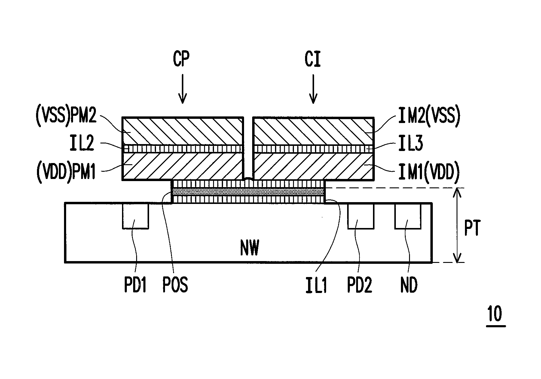
[0021]References will now be made in detail to the exemplary embodiments of the invention, examples of which are illustrated in the accompanying drawings. Wherever possible, the same reference numbers are used in the drawings and the description to refer to the same or like parts.

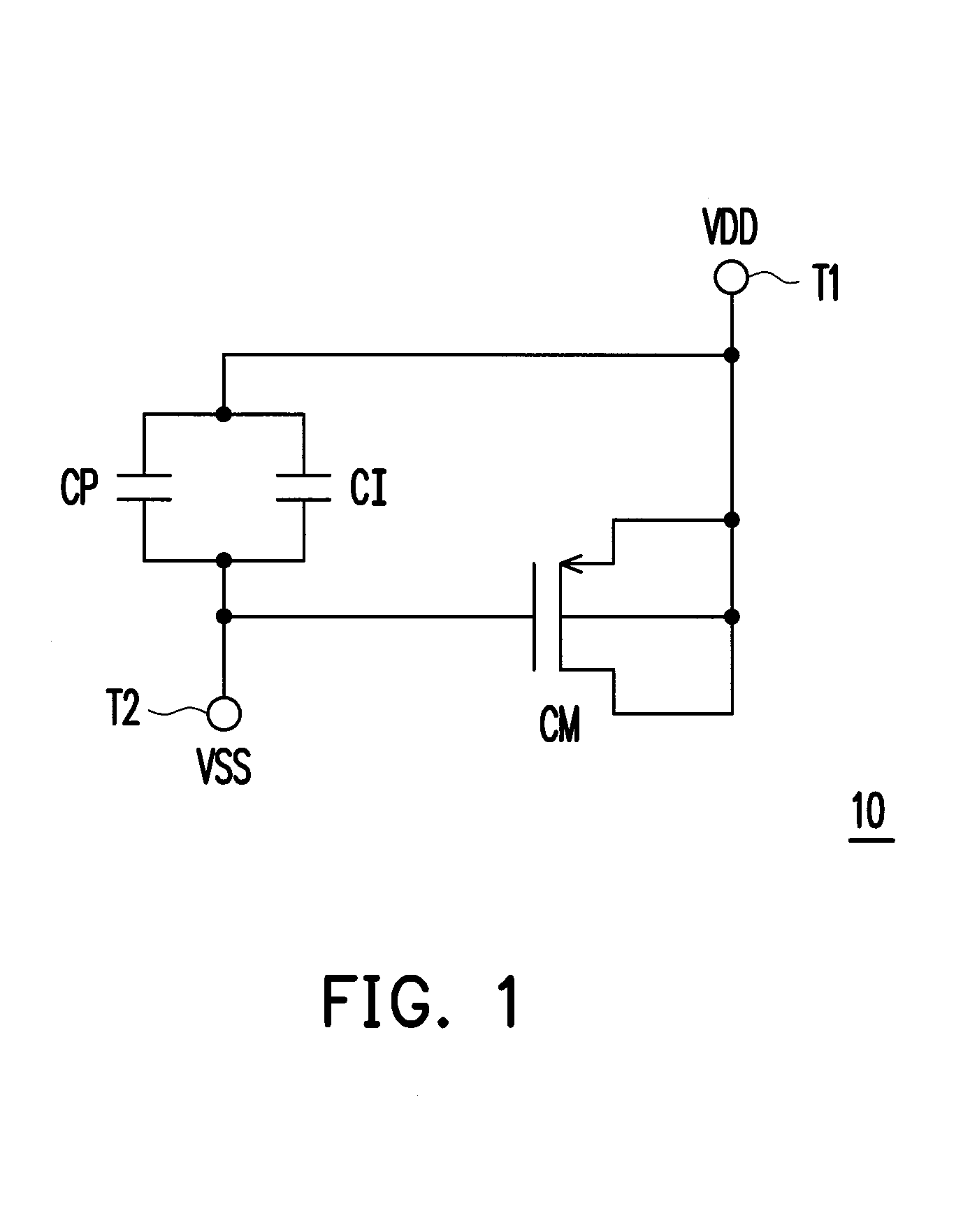
[0022]FIG. 1 is an equivalent circuit diagram illustrating a capacitor structure 10 applied to an integrated circuit (IC) according to an embodiment of the invention. With reference to FIG. 1, the capacitor structure 10 includes a metal-oxide semiconductor (MOS) capacitor CM and two metal capacitors CP and CI both with different structures. The MOS capacitor CM has a first terminal T1 and a second terminal T2. The first terminal T1 may be coupled to a first voltage, e.g., a system voltage VDD or a positive supply voltage. The second terminal T2 may be coupled to a second voltage, e.g., a ground voltage VSS or a negative supply voltage. Namely, compared to the voltage coupled to the second terminal T2, the v...


PUM


Abstract

A capacitor structure applied to an integrated circuit (IC) is provided. The capacitor structure includes a metal-oxide semiconductor (MOS) capacitor and two metal structures with different structures. The MOS capacitor has a first terminal and a second terminal. The two metal capacitors are formed above the MOS capacitor and respectively coupled between the first terminal and the second terminal. Subject to the confined chip area, the capacitance of the above-mentioned capacitor structure can still reach the design value, and the above-mentioned capacitor structure is further characterized by a large amount of current flow.

Description

CROSS-REFERENCE TO RELATED APPLICATION[0001]This application claims the priority benefit of Taiwan application serial no. 100132139, filed on Sep. 6, 2011. The entirety of the above-mentioned patent application is hereby incorporated by reference herein and made a part of this specification.BACKGROUND OF THE INVENTION[0002]1. Technology Field[0003]The present invention generally relates to a semiconductor structure, and more particularly to a capacitor structure applied to an integrated circuit (IC).[0004]2. Description of Related Art[0005]With the increase in the level of integration of the semiconductor device, dimensions of the device are gradually reduced. Hence, space occupied by the capacitor is relatively reduced because the available chip area of the capacitor plate is forced to decrease. This leads to reduction of the capacitance of the capacitor. After entry into the deep sub-micron fabrication phase, the issue of the capacitance reduction of the capacitor becomes more ser...

Claims


Application Information

Patent Timeline
Patent Type & Authority Patents(United States)
IPC IPC(8): H01L27/108H01L23/522H01L29/94H01L27/01H01L49/02
CPCH01L29/94H01L23/5223H01L27/016H01L28/60H01L2924/0002
Inventor CHEN, TIEN-LUNG
Owner PHISON ELECTRONICS
Why Eureka
Try Eureka