Organic light emitting diode device and method for fabricating the same

a light-emitting diode and organic technology, applied in the direction of solid-state devices, electric lighting sources, electric light sources, etc., can solve the problems of degrading quality of the inorganic insulating layer such as the passivation layer disposed on the oled device, and achieve the effect of improving the reliability of the environmen

Active Publication Date: 2016-04-12
LG DISPLAY CO LTD
View PDF18 Cites 10 Cited by
  • Summary
  • Abstract
  • Description
  • Claims
  • Application Information

AI Technical Summary

Benefits of technology

[0040]Therefore, an aspect of the detailed description is to provide an organic light-emitting diode (OLED) device capable of having an enhanced environment reliability by preventing moisture from being introduced into an active area from outside, by forming moisture blocking portions at a planarization layer in a non-active area, and a method for fabricating the same.
[0044]Firstly, owing to the moisture blocking portions formed at the planarization layer in the non-active area, foreign materials or moisture generated from the first passivation layer, the second passivation layer, etc. due to occurrence of a crack can be prevented from being introduced into the active area.
[0045]Foreign materials or moisture inside the planarization layer, which may cause degradation of organic materials inside a light-emitting region, can be outgassed through the anode holes formed at the auxiliary electrode pattern disposed in the non-active area. The anode holes, through which the planarization layer and the bank are connected to each other, may serve as a path through which moisture introduced from outside flows to the active area (AA). However, even if moisture introduced from outside flows through the anode holes, the moisture can be prevented from moving to the active area (AA) by the moisture blocking portions of the planarization layer formed below the auxiliary electrode pattern. This can allow a top emission type OLED device adopting a face seal structure, to have an enhanced environment reliability.

Problems solved by technology

However, the conventional OLED device may have the following problems.
However, in this case, an inorganic insulating layer such as the passivation layer disposed on the OLED device has a degraded quality due to a stair-shaped portion.
Secondly, when a defect occurs in the face seal structure, e.g., the barrier film, the adhesive, etc., moisture (H2O) is rapidly introduced into the active area (AA) through a bank.
However, in this case, moisture may spread through a planarization layer to cause a problem.

Method used


Image

  • Organic light emitting diode device and method for fabricating the same
  • Organic light emitting diode device and method for fabricating the same
  • Organic light emitting diode device and method for fabricating the same

Examples


Embodiment Construction

[0055]Description will now be given in detail of the exemplary embodiments, with reference to the accompanying drawings. For the sake of brief description with reference to the drawings, the same or equivalent components will be provided with the same reference numbers, and description thereof will not be repeated.

[0056]An organic light emitting diode (OLED) device according to the present invention is categorized into a top emission type and a bottom emission type according to a propagation direction of emitted light. Hereinafter, a top emission type OLED device will be explained.

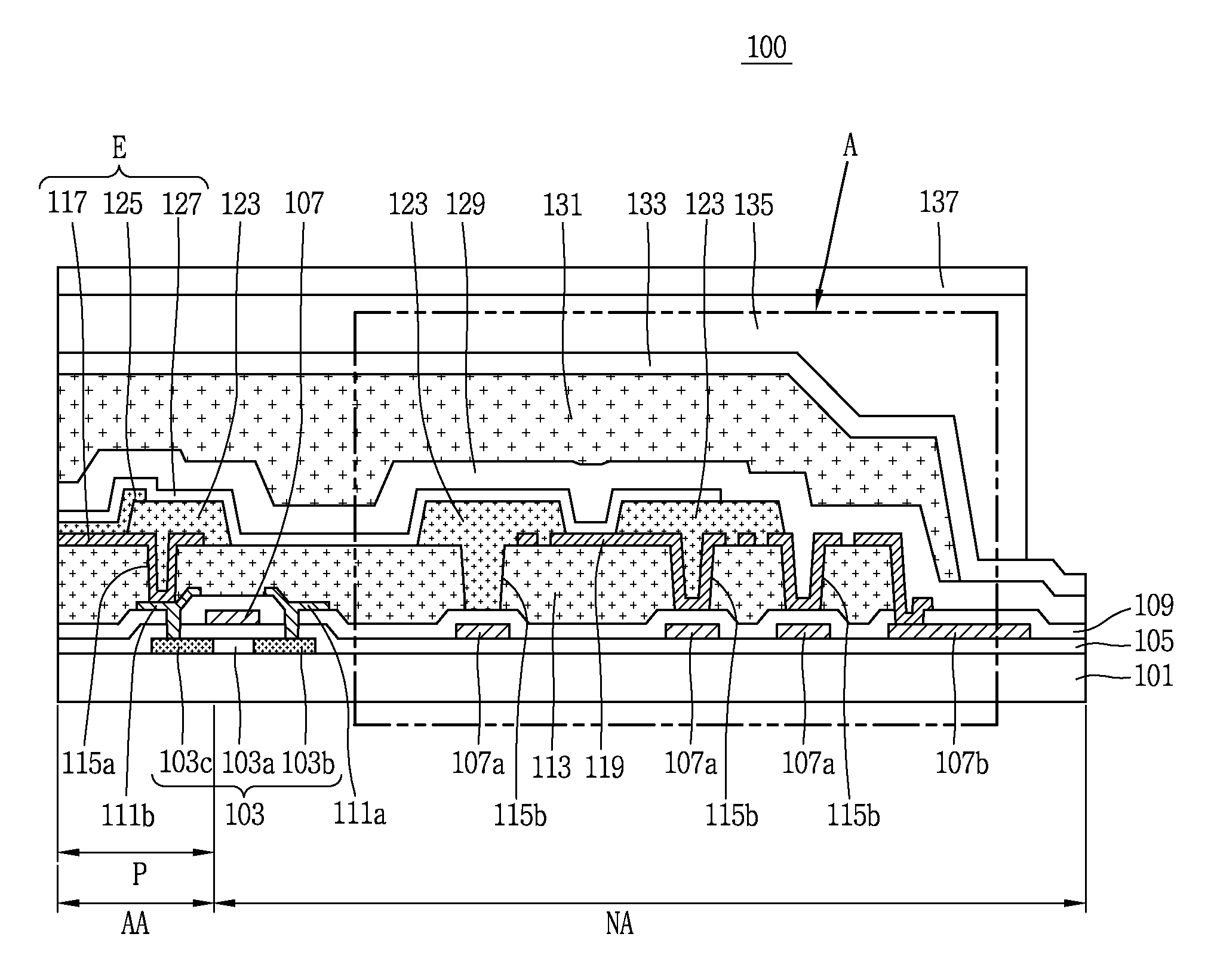
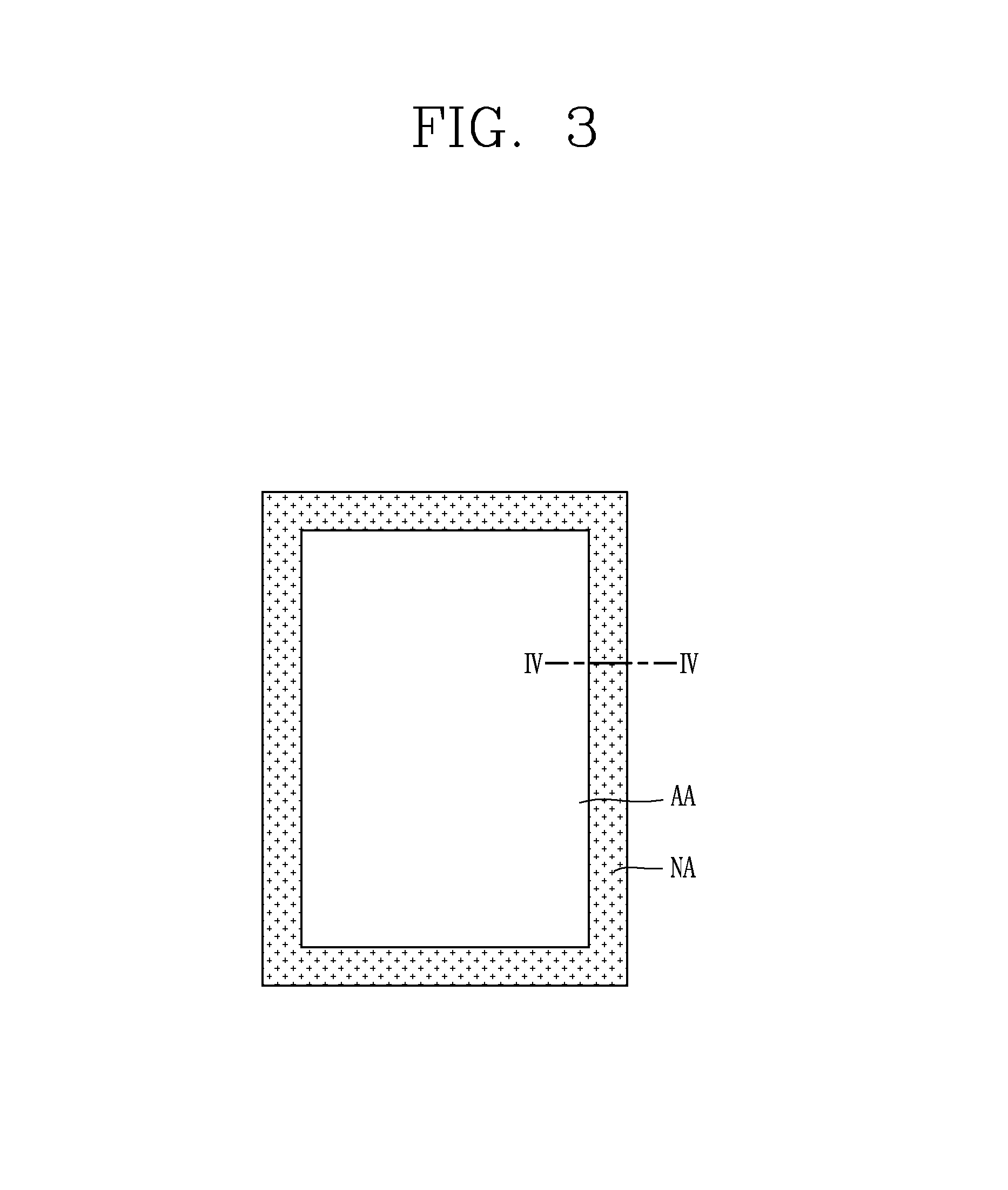
[0057]FIG. 3 is a planar view schematically illustrating an OLED device according to the present invention, FIG. 4 is a sectional view taken along line ‘IV-IV’ in FIG. 3, which schematically illustrates an OLED device according to the present invention, and FIG. 5 is an enlarged sectional view of part ‘A’ in FIG. 4, which illustrates that introduction of moisture from a moisture blocking portion of a plana...


PUM


Abstract

Disclosed are an organic light emitting diode device, and a method for fabricating the same. The organic light emitting diode device comprises a non-active area formed outside an active area of a substrate; a switching thin film transistor and a driving thin film transistor at each of the pixel regions; a planarization layer on the substrate; a first electrode on the planarization layer; a bank formed in the non-active area outside each pixel region; an organic light emitting layer on the first electrode; a second electrode on an entire surface of the substrate; a first passivation layer on the substrate; an organic layer on the first passivation layer; a second passivation layer on the organic layer and the first passivation layer; a barrier film disposed to face the substrate.

Description

CROSS-REFERENCE TO RELATED APPLICATION[0001]Pursuant to 35 U.S.C. §119(a), this application claims the benefit of earlier filing date and right of priority to Korean Application No. 10-2012-0142202, filed on Dec. 7, 2012, the contents of which is incorporated by reference herein in its entirety.BACKGROUND OF THE DISCLOSURE[0002]1. Field of the Disclosure[0003]The present disclosure relates to an organic light emitting diode device (hereinafter, will be referred to as “OLED” device), and particularly, to an OLED device capable of having an enhanced environment reliability by preventing moisture from being introduced thereinto from outside, and a method for fabricating the same.[0004]2. Background of the Disclosure[0005]An organic light-emitting diode (OLED) device, one of flat panel display devices, has high brightness and a low operation voltage. Further, the OLED device has a high contrast ratio because it is a spontaneous light-emitting type, and it can implement a display of an u...

Claims


Application Information

Patent Timeline
Patent Type & Authority Patents(United States)
IPC IPC(8): H01L35/24H01L51/52H01L27/32
CPCH01L27/3246H01L27/3262H01L51/5256H01L51/5212H01L51/5253H01L27/3276H01L27/3258H01L27/3248H01L51/56H01L27/3244H01L2227/323H01L27/1259H01L27/124H01L27/1248H10K59/12H10K50/8445H10K59/1201H05B33/04H10K59/1213H10K50/814H10K50/844H10K59/122H10K59/123H10K59/124H10K59/131H10K71/00
Inventor LEE, JINOSONG, SANGMOOKIM, JUNGCHULNA, SEHWANKIM, JIYUNHASUMI, TARO
Owner LG DISPLAY CO LTD
Why Eureka
Try Eureka