
Package structure

a packaging and structure technology, applied in the direction of semiconductor devices, electrical equipment, semiconductor/solid-state device details, etc., can solve the problems of difficult to meet the requirements mechanical and electrical connections between the chip and the substrate, etc., to achieve the effect of reducing the overall thickness of the package structure and facilitating the requirement of low-profile package structur

Active Publication Date: 2016-04-26
POWERTECH TECHNOLOGY
View PDF2 Cites 1 Cited by
  • Summary
  • Abstract
  • Description
  • Claims
  • Application Information

AI Technical Summary

Benefits of technology

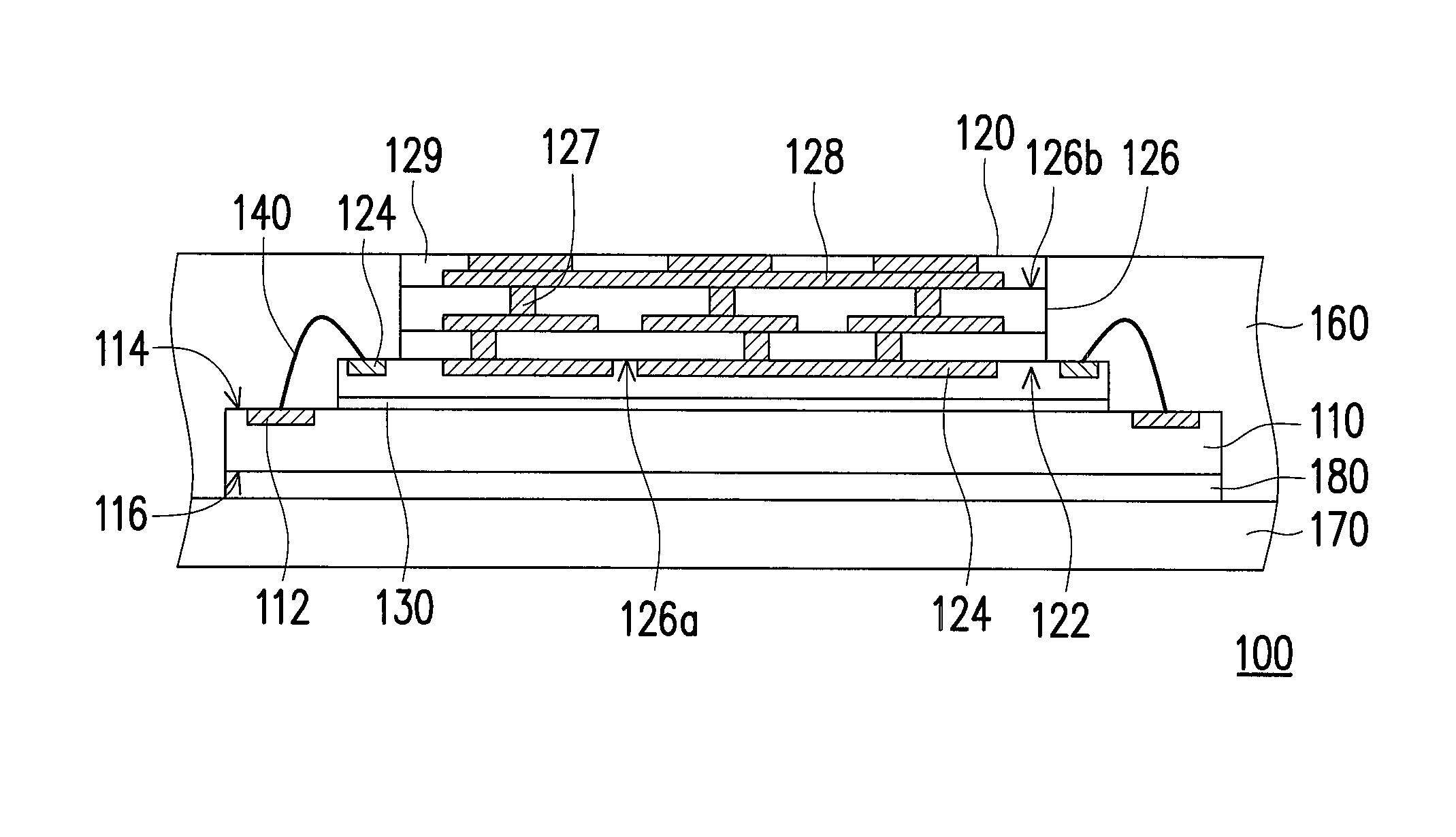
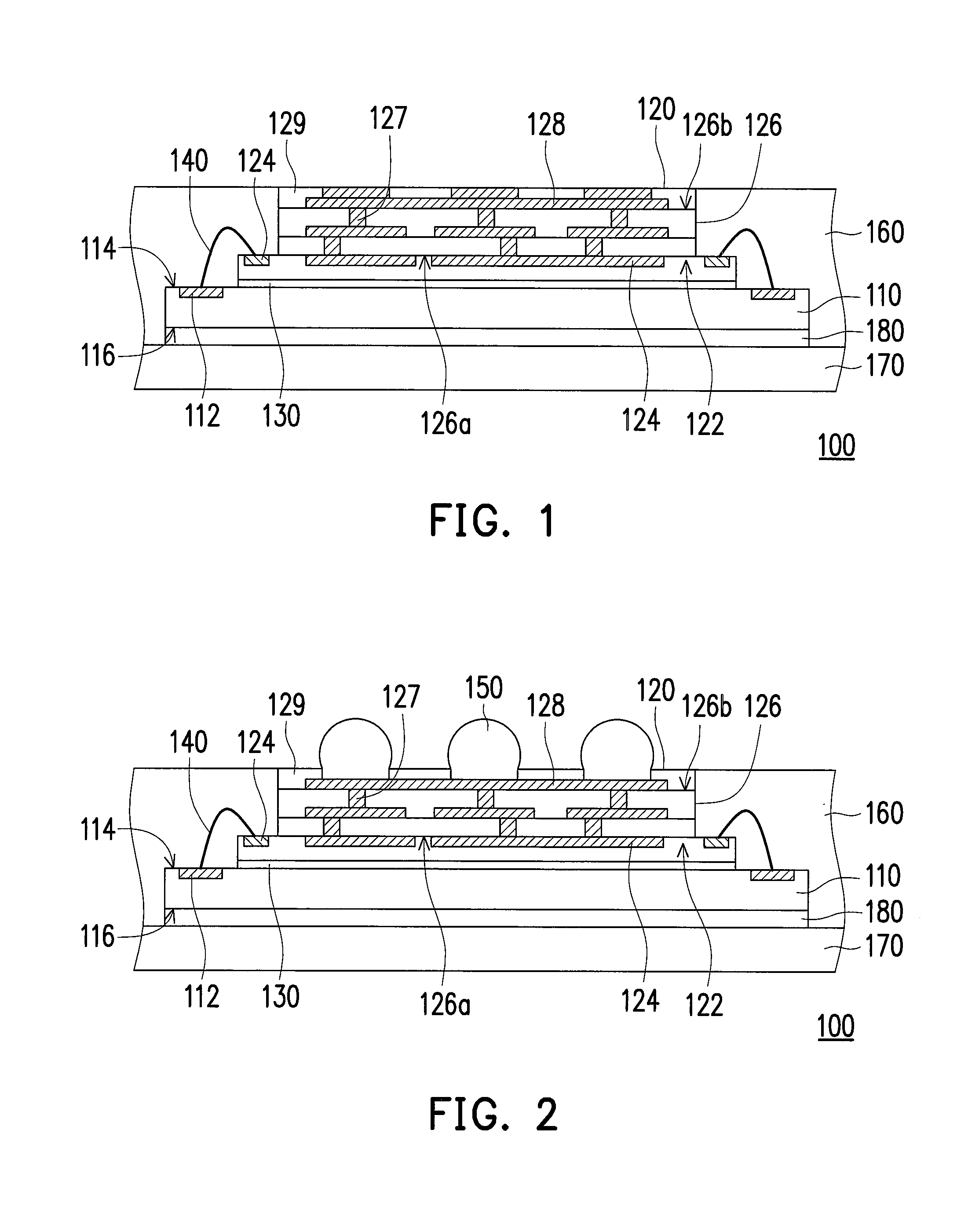
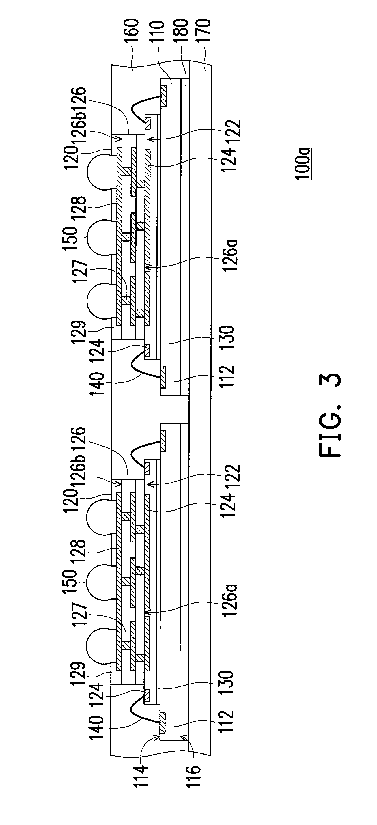
The package structure of the invention has a reduced thickness and meets the requirements of low-profile package structure. The substrate is placed on the chip, exposing the bonding pads, and includes a first solder mask, a first patterned circuit layer, and a core layer. A wire is connected between the first patterned circuit layer and the bonding pads, and the level of each wire is lower than the substrate surface level. The molding compound can cover the wires without giving additional thickness to the package structure, as long as the molding compound is coplanar with the substrate surface.

Problems solved by technology

The mechanical and electrical connections between the chip and the substrate have posed challenges for chip designers.
Therefore, the package structure using wire bonding process is hard to meet the low-profile requirements.

Method used


Image

  • Package structure
  • Package structure
  • Package structure

Examples


Embodiment Construction

[0027]In the following detailed description of the preferred embodiments, reference is made to the accompanying drawings which form a part hereof, and in which are shown by way of illustration specific embodiments in which the invention may be practiced. In this regard, directional terminology, such as “top”, “bottom”, “front”, “back”, etc., is used with reference to the orientation of the Figure(s) being described. The components of the invention can be positioned in a number of different orientations. As such, the directional terminology is used for purposes of illustration and is in no way limiting. It is to be understood that the phraseology and terminology used herein are for the purpose of description and should not be regarded as limiting. The use of “including,”“comprising,” or “having” and variations thereof herein is meant to encompass the items listed thereafter and equivalents thereof as well as additional items. On the other hand, the drawings are only schematic and the...


PUM


Abstract

A package structure includes a chip, a substrate, wires and a molding compound. The chip includes an active surface, a back surface and bonding pads disposed on the active surface. The substrate includes first and second solder masks, first and second patterned circuit layers and a core layer having a first surface and a second surface. The first patterned circuit layer is disposed on the first solder mask. The core layer disposed on the first solder mask with the first surface partially exposes the first patterned circuit layer. The substrate disposed on the active surface with the first solder mask exposes the bonding pads. The second patterned circuit layer disposed on the second surface. The second solder mask partially covers the second patterned circuit layer. The wires are connected between the first patterned circuit layer and the bonding pads. The molding compound covers the chip, the wire and the substrate.

Description

BACKGROUND OF THE INVENTION[0001]1. Field of the Invention[0002]The present invention generally relates to a package structure. More particularly, the present invention relates to a package structure of a chip.[0003]2. Description of Related Art[0004]Modern electronic equipment relies heavily on printed circuit boards on which semiconductor chips, or integrated circuits (ICs), are mounted. The mechanical and electrical connections between the chip and the substrate have posed challenges for chip designers. Three well known techniques for interconnecting the IC to the substrate are: wire bonding, tape automated bonding (TAB) and flip-chip.[0005]A wire bonding technology is a common chip packaging technology applied to electrically connect a chip to a substrate. Here, the substrate is, for example, a circuit board. Generally, the wire bonding technology includes forming a stud bump in a wire bonding pad region of the substrate with use of a stud bump machine and extending wires upward...

Claims


Application Information

Patent Timeline
Patent Type & Authority Patents(United States)
IPC IPC(8): H01L23/02H01L23/522H01L23/00
CPCH01L23/5226H01L24/49H01L2924/183H01L23/49816H01L23/49822H01L23/49827H01L2924/181H01L2924/00014H01L2224/73265H01L2924/14H01L2224/73215H01L2224/48091H01L2224/32225H01L24/32H01L2924/15311H01L24/48H01L24/73H01L24/97H01L2224/32014H01L24/33H01L2224/33181H01L23/3128H01L21/568H01L2924/00012H01L2224/45099H01L2224/29099H01L2224/05599
Inventor FAN, WEN-JENG
Owner POWERTECH TECHNOLOGY
Learn More