
Ultraviolet avalanche photodetector based on absorption and multiplication layer separation of hetero-structure

A technology of photodetectors and heterostructures, applied in the field of ultraviolet detectors, which can solve the problems of increased process complexity, surface degradation of epitaxial layers, and n-type GaN growth, so as to reduce the difficulty of testing, avoid rigid requirements, and simplify the process flow Effect

Inactive Publication Date: 2014-07-09
SUN YAT SEN UNIV
View PDF3 Cites 0 Cited by
  • Summary
  • Abstract
  • Description
  • Claims
  • Application Information

AI Technical Summary

Problems solved by technology

[0005] For GaN avalanche photodetectors with traditional PIN structure and absorption multiplication separation (SAM) structure, due to the memory effect of the p-type GaN doping element Mg and the growth of heavily doped p-type GaN, the surface of the epitaxial layer will deteriorate, resulting in It is difficult to grow n-type GaN with good crystalline quality on top of p-type GaN, so a back-incidence method is required to achieve hole-triggered avalanche gain
However, since the back-incidence requires the substrate to be transparent, the substrate needs to be thinned and polished on both sides, which increases the complexity of the process.
In addition, the back-incident ultraviolet light signal must pass through the substrate and buffer layer before reaching the absorbing layer (or active layer). During this process, the incident light will be absorbed and scattered, resulting in a decrease in the external quantum efficiency of the detector.
If the AlGaN material with a wider band gap is used as the buffer layer, the lattice and thermal mismatch between the AlGaN epitaxial layer and the substrate will be more serious than that of the GaN epitaxial layer, resulting in the AlGaN buffer layer and the active growth on it. High-density defects in the layer will degrade the key performance of the device, such as dark current, quantum efficiency, etc.

Method used


Image

  • Ultraviolet avalanche photodetector based on absorption and multiplication layer separation of hetero-structure

Examples


Embodiment Construction

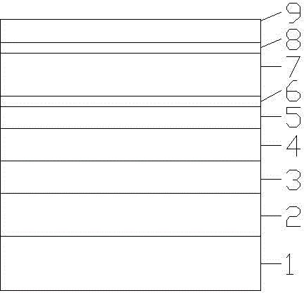
[0012] Such as figure 1 As shown, an ultraviolet avalanche photodetector based on heterostructure absorption and multiplication layer separation, wherein the device includes a substrate 1, which is grown sequentially by epitaxial growth methods such as molecular beam epitaxy or metal organic chemical vapor deposition epitaxy 25nm low-temperature GaN buffer layer and 2μm high-temperature non-doped GaN buffer layer 2 grown on substrate 1, 1μm thick n-type doped GaN layer 3, 0.2μm thick non-doped or low-doped intrinsic GaN absorption layer 4, 50nm thick n-type GaN layer with low doping concentration 5, 10nm thick n-type Al with low doping concentration x Ga 1-x N (x=0-0.2) composition graded layer 6, 0.2 μm thick non-doped intrinsic Al 0.2 Ga 0.8 N multiplication layer 7, 10nm thick p-type doped Al- y Ga 1-y N (y=0.2-0) composition graded layer 8, p-type doped GaN layer 9 with a thickness of 0.1 μm. The multiplication layer 7 acts as a window at the same time, allowing the ...


PUM


Abstract

The invention relates to an ultraviolet detector, and particularly relates to an ultraviolet avalanche photodetector based on absorption and multiplication layer separation of a hetero-structure. The photodetector comprises a substrate, and a buffer layer, an n-type doped GaN layer, a non-doped or low-doping-concentration intrinsic GaN absorption layer, a low-doping-concentration n-type GaN layer and a low-doping-concentration n-type AlGaN component slow-variation layer, a non-doping intrinsic AlxGal-xN multiplication layer, a p-type doped AlGaN component slow-variation layer and a p-type doped GaN layer, which grow on the substrate in sequence. The ultraviolet avalanche photodetector provided by the invention has the advantages of low noise, high gain and high performance. Due to the special structure of the photodetector, a front incident single can realize the avalanche gain of hole triggering, thereby smartly avoiding rigid requirement of conventional back incidence, simplifying the process flow and reducing the test difficulty.

Description

technical field [0001] The invention relates to an ultraviolet detector, in particular to an ultraviolet avalanche photodetector based on heterostructure absorption and multiplication layer separation. Background technique [0002] Compound semiconductor gallium nitride (GaN) belongs to the third generation of semiconductor materials, with direct band gap, large band gap (3.43eV), high electron drift saturation speed, small dielectric constant, high temperature resistance, corrosion resistance, radiation resistance, heat conduction With good performance and other characteristics, it is an ideal material for making short-wavelength optoelectronic devices and high-power, high-frequency electronic devices with high quantum efficiency, high-density integration and resistance to harsh environments. [0003] Ultraviolet detection technology is widely used in military, civil and scientific research, such as missile plume detection, flame detection, environmental monitoring, space c...

Claims


Application Information

Patent Timeline
Patent Type & Authority Patents(China)
IPC IPC(8): H01L31/107H01L31/0352H01L31/076
CPCY02E10/50Y02E10/548
Inventor 江灏黄泽强
Owner SUN YAT SEN UNIV
Learn More