Supercharge Your Innovation With Domain-Expert AI Agents!

Fabricating method of thin film transistor, thin film transistor and display panel

a thin film transistor and fabrication method technology, applied in transistors, electrical devices, semiconductor devices, etc., can solve the problems of low carrier mobility within polycrystalline silicon, and achieve the effect of improving the stability of thin film transistors fabricated by this method, simple and easy to implemen

Active Publication Date: 2016-04-26
BOE TECH GRP CO LTD +1
View PDF17 Cites 0 Cited by
  • Summary
  • Abstract
  • Description
  • Claims
  • Application Information

AI Technical Summary

Benefits of technology

The method significantly improves carrier mobility and stability of thin film transistors by aligning polycrystalline silicon grains vertically, reducing defects and enhancing energy transfer efficiency.

Problems solved by technology

These grains formed in the spontaneous conditions are small in size with random shapes and arrangements, causing low carrier mobility within the polycrystalline silicon.

Method used


Image

  • Fabricating method of thin film transistor, thin film transistor and display panel
  • Fabricating method of thin film transistor, thin film transistor and display panel
  • Fabricating method of thin film transistor, thin film transistor and display panel

Examples


Embodiment Construction

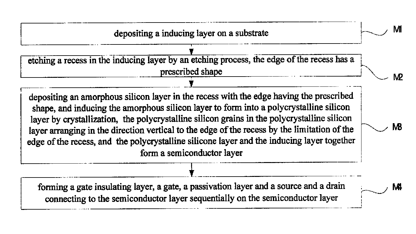
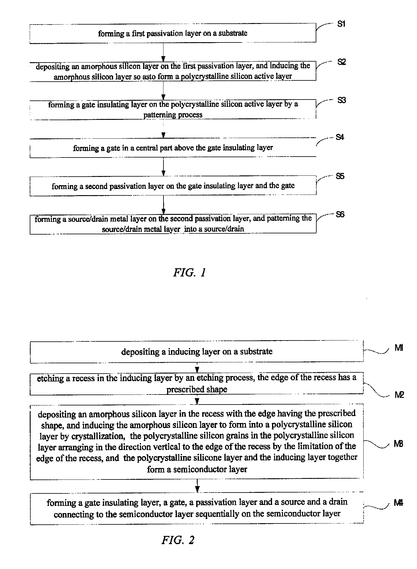
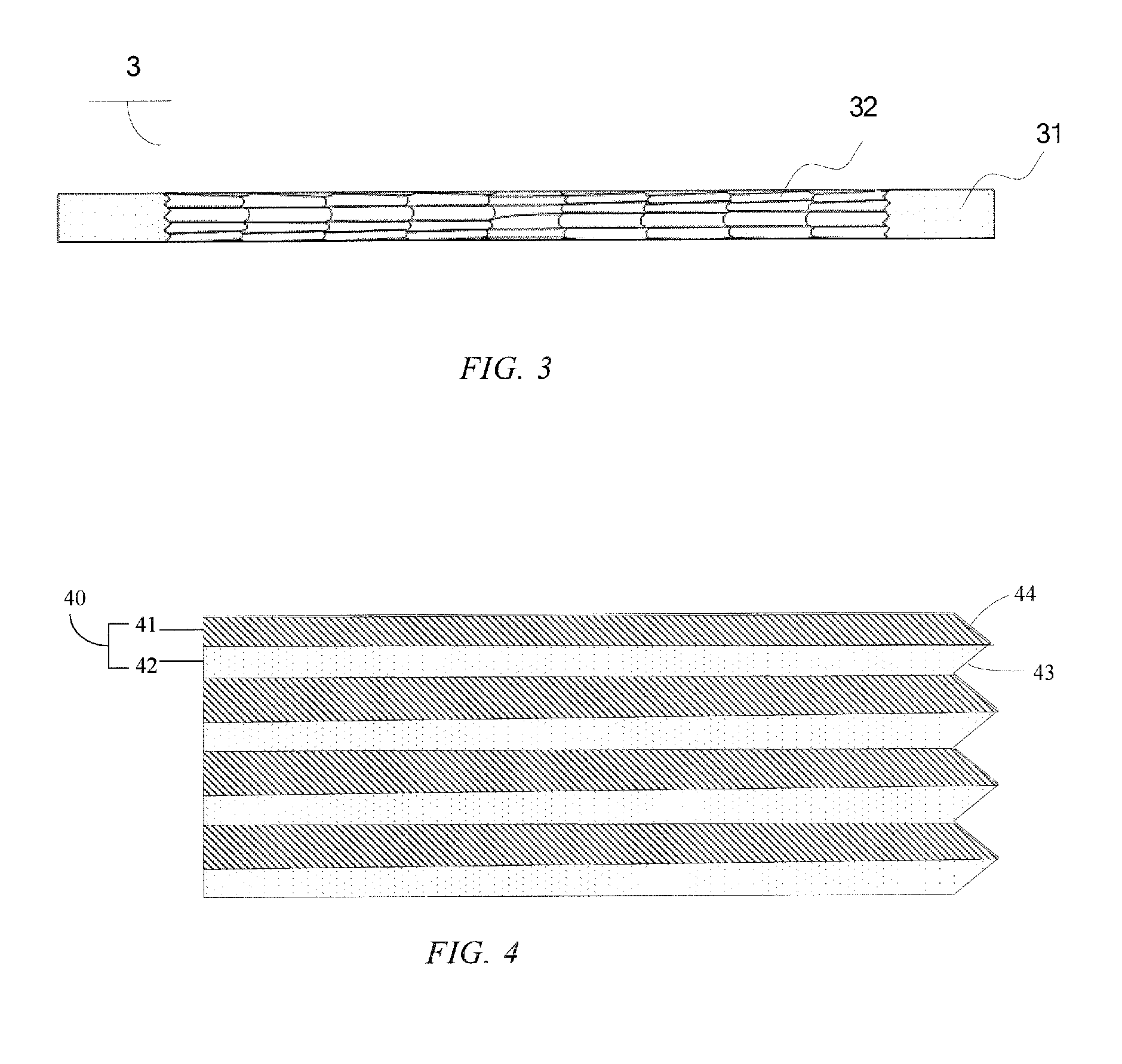
[0022]The technical solution of the embodiments of the present disclosure will be described clearly and fully in connection with the drawings of the embodiments of the present disclosure. It is obvious that the described embodiments are just a part but not all of the embodiments of the present disclosure. Based on the described embodiments of the present disclosure, those skilled in the art can obtain all other embodiment without any inventive work, which all fall into the scope of the claimed invention.

[0023]Unless otherwise defined, technical terms or scientific terms used herein shall have a common meaning known by those skilled in the art of the present disclosure. Words and expressions such as “first”, “second” and the like used in the description and claims of the patent application of the present disclosure do not denote any sequence, quantity or significance, but distinguish different components. Likewise, words such as “a”, “an” and the like do not denote quantitative restr...


PUM

PropertyMeasurementUnit
thicknessaaaaaaaaaa
carrier mobilityaaaaaaaaaa
shapeaaaaaaaaaa

Abstract

Embodiments of the invention provide a fabricating method a thin film transistor, a thin film transistor and a display panel, so as to improve carrier mobility in the polycrystalline silicon. The fabricating method a thin film transistor comprises following M1, depositing an inducing layer on a substrate; M2, etching a recess in the inducing layer by an etching process, the recess having an edge with a prescribed shape; M3, depositing an amorphous silicon layer in the recess having an edge with a prescribed shape, and inducing the amorphous silicon layer to form a polycrystalline silicon layer by crystallization method, polycrystalline silicon grains in the polycrystalline silicon layer arranging in a direction vertical to the edge of the recess by the limitation of the edge of the recess, and the polycrystalline silicone layer and the inducing layer together forming a semiconductor layer; and M4, forming a gate insulating layer, a gate, a passivation layer and a source and a drain connecting with the semiconductor layer sequentially on the semiconductor layer.

Description

FIELD[0001]The invention relates to liquid crystal display field, in particular relates to a fabricating method of a thin film transistor, a thin film transistor and a display panel.BACKGROUND[0002]Recently, with the development of the technology of polycrystalline silicon thin film transistor (TFT), there are more applications of the TFT, and the polycrystalline silicon thin film transistor is considered to be an ideal alternative of an amorphous silicon thin film transistor. In comparison with the amorphous silicon thin film transistor, the polycrystalline silicon thin film transistor has the characteristics of high mobility, high integration, high resolution and so on, thus providing a brighter and finer image.[0003]A thin film transistor known by inventors is usually fabricated by a following method. Referring to FIG. 1, the method comprises: step S1, forming a first passivation layer on a substrate; step S2, depositing an amorphous silicon layer on the first passivation layer, ...

Claims


Application Information

Patent Timeline
Patent Type & Authority Patents(United States)
IPC IPC(8): H01L21/00H01L21/20H01L27/092H01L29/786H01L21/02H01L29/66H01L21/311
CPCH01L29/66757H01L29/78675H01L27/1281H01L21/0217H01L21/02532H01L21/02592H01L21/02672H01L21/31111H01L29/78603H01L21/02658H01L21/02667H01L29/04
Inventor LI, JINGXIE, ZHENYUCHEN, XUZHANG, WENYUXU, DA
Owner BOE TECH GRP CO LTD
Features
  • R&D
  • Intellectual Property
  • Life Sciences
  • Materials
  • Tech Scout
  • Unparalleled Data Quality
  • Higher Quality Content
  • 60% Fewer Hallucinations
Learn More