Organic light emitting display device

a light-emitting display and organic technology, applied in the direction of semiconductor/solid-state device manufacturing, semiconductor devices, electrical devices, etc., can solve the problems of deterioration of the brightness of the organic light-emitting diodes, and achieve the effects of enhancing high temperature reliability, expanding life time, and enhancing light efficiency

Active Publication Date: 2016-04-26
LG DISPLAY CO LTD
View PDF5 Cites 2 Cited by
  • Summary
  • Abstract
  • Description
  • Claims
  • Application Information

AI Technical Summary

Benefits of technology

[0022]The embodiments are to provide an organic light emitting display device which is adapted to enhance the light efficiency and expand the life time by preventing an overlap between a peak charge density position and a peak recombination position within an organic emission layer using difference between hole mobility of a hole transport layer of an organic light emitting diode and electron mobility of an electron transport layer of the organic light emitting diode.
[0023]Also, the embodiments are to provide an organic light emitting display device which allows a recombination region of an organic emission layer to be enlarged toward a high charge density region by a difference between hole mobility of the hole transport layer and electron mobility of an electron transport layer when an organic light emitting diode is driven so that high temperature reliability is enhanced and the life time of elements is expanded.

Problems solved by technology

Due to this, the brightness of the organic light emitting diode also deteriorates after the high temperature reliability inspection.

Method used


Image

  • Organic light emitting display device
  • Organic light emitting display device
  • Organic light emitting display device

Examples


first embodiment

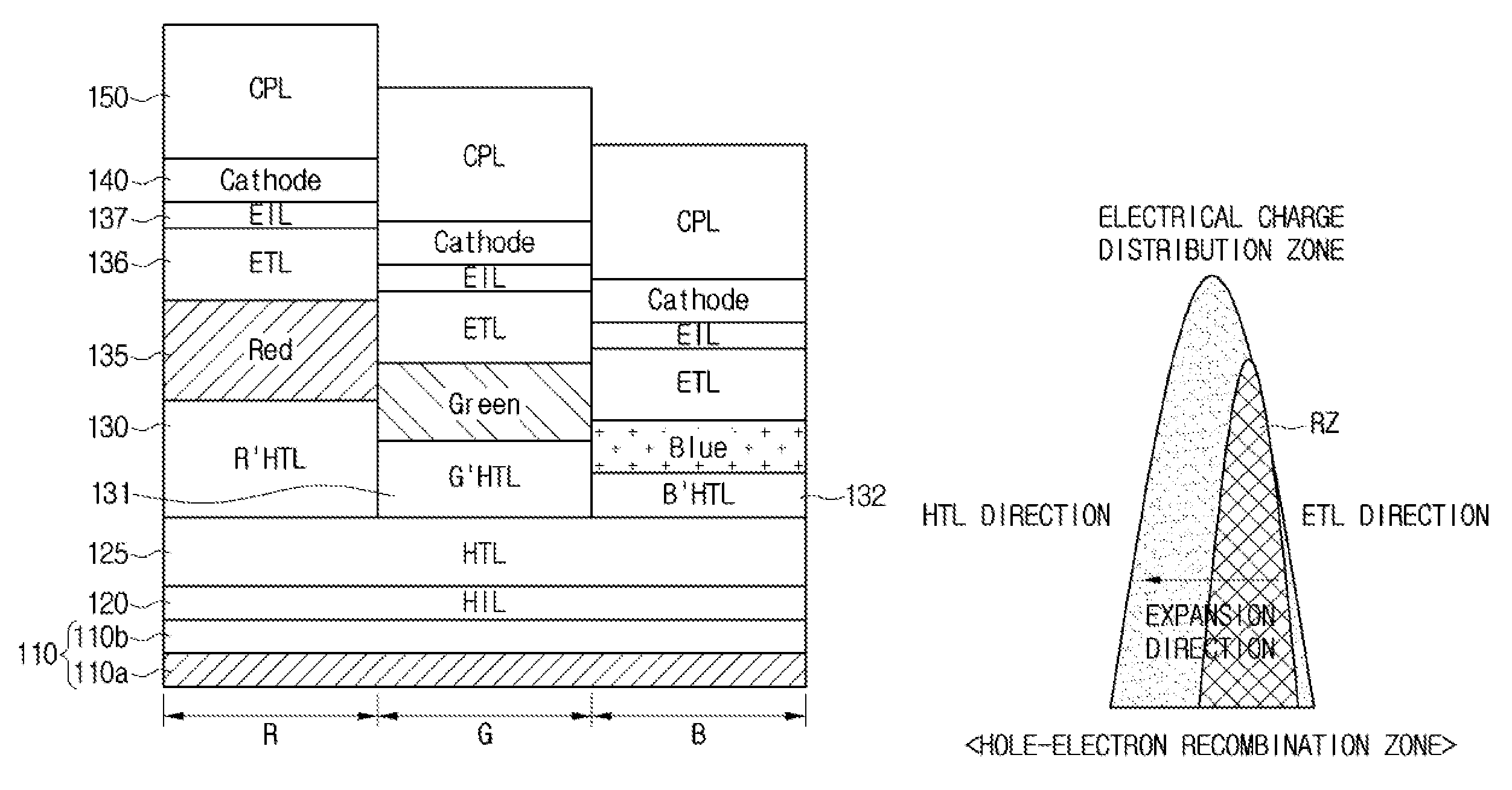
[0048]FIG. 4 is a cross-sectional view showing a structure of an organic light emitting display device according to the present disclosure.

[0049]Referring to FIG. 4, the organic light emitting display device according to a first embodiment of the present disclosure includes a first electrode 110 formed on a substrate, which is defined into red, green and blue sub-pixel regions, and used as a reflective electrode. Also, the organic light emitting display device includes a hole injection layer (HIL) 120 and a first hole transport layer (HTL) 125 stacked on the first electrode 110 corresponding to all the red, green and blue sub-pixel regions.

[0050]The first electrode 110 can be used as an anode electrode of an organic light emitting diode. Also, the first electrode 110 can be formed by stacking a second metal layer 110b of a transparent conductive material on a first metal layer 110a with high reflectance. The first metal layer 110a can be formed from one of aluminum Al and silver Ag....

second embodiment

[0092]Referring to FIGS. 12, 13A and 13B, the organic light emitting display device according to the present disclosure allows a first electrode 210 to be formed on the entire surface of a substrate which is defined into red, green and blue regions. The first electrode 210 can be formed in a stacked structure of a first metal layer 210a and a second metal layer 210b. A hole injection layer (HIL) 220 and a first hole transport layer (HTL) 225 each corresponding to all the red, green and blue regions are stacked on the first electrode 210.

[0093]The hole injection layer 220 can be formed of one selected from a material group which includes arylamine based compounds, such as NATA, 2T-NATA and NPNPB, and p-doped materials such as F4-TCNQ and PPDN, but it is not limited to this.

[0094]The first hole transport layer (HTL) 225 can be formed of one selected a material group of arylamine based compounds, starburst-aromatic-amine-based-materials, spiro-ladder type materials, NPD (N,N-dinaphthyl...


PUM


Abstract

An organic light emitting display device is disclosed which includes: a first electrode including red, green and blue sub-pixel regions; a first hole injection layer disposed on the first electrode; a first hole transport layer disposed on the hole injection layer; second, third and fourth hole transport layers arranged on the first hole transport layer corresponding to the red, green and blue regions, respectively; an organic emission layer disposed on the second, third and fourth hole transport layers; an electron transport layer disposed on the organic emission layer; and a second electrode disposed on the electron transport layer, the second, third and fourth hole transport layers each having a hole mobility different from an electron mobility of the electron transport layer.

Description

CROSS-REFERENCE TO RELATED APPLICATION[0001]The present application claims priority to and the benefit under 35 U.S.C. §119(a) of Korean Patent Application No. 10-2013-0169365 filed on Dec. 31, 2013, which is hereby incorporated by reference for all purposed as if fully set forth herein.BACKGROUND OF THE INVENTION[0002]1. Field of the Disclosure[0003]The present application relates to an organic light emitting display device. More particularly, the present application relates to an organic light emitting display device adapted to enhance high temperature reliability and expand life time of elements by adjusting hole and electron mobilities of a hole transport layer and an electron transport layer which are formed in an organic light emitting diode.[0004]2. Description of the Related Art[0005]An organic light emitting diode used in an organic light emitting display device is a self-luminous element which includes an emission layer formed between two electrodes. The organic light emit...

Claims


Application Information

Patent Timeline
Patent Type & Authority Patents(United States)
IPC IPC(8): H01L31/12H01L27/32H01L51/50
CPCH01L51/5064H01L27/3211H01L51/508H01L51/5004H10K59/35H10K50/11H10K2101/40H10K50/156H10K50/16H10K2101/00H10K50/15H10K50/166
Inventor KIM, HO SUNGKIM, KWANG HYUN
Owner LG DISPLAY CO LTD
Why Eureka
Try Eureka