Photolithographic masks and fabrication method thereof

a technology of photolithography and masks, applied in the field of semiconductor manufacturing technology, can solve the problems of affecting the pattern on the wafer may not be exactly identical to the pattern on the mask, and the deformation and deviation of the pattern formed by the photolithography process are becoming more and more severe, so as to achieve the effect of improving the performance and yield of the ics

Active Publication Date: 2016-05-24
SEMICON MFG INT (SHANGHAI) CORP
View PDF2 Cites 0 Cited by
  • Summary
  • Abstract
  • Description
  • Claims
  • Application Information

AI Technical Summary

Benefits of technology

[0014]Another aspect of the present disclosure includes a method for fabricating a photolithographic mask. The method includes providing substrate having a first surface configured as a light incidence plane and a second face. The method also includes forming a plurality of scattering centers functioning as a refractive index disturbance inside the substrate. Further, the method includes forming a plurality of mask patterns on the second surface of the substrate.
[0029]Various factors may achieve the adjustment of the scattering centers 302 to the light intensity. One factor may be a reflection effect of the scattering assisting patterns 302. The scattering centers 302 may reflect a portion of the incidence light, thus incidence light under (or behind) the scattering centers 302 is reduced. Another factor may be a projection the scattering assisting patterns 302 on a plane of the mask patterns 301. The projection may adjust a light intensity distributed on the mask patterns 301. Such an adjustment may reduce intensity differences of the mask patterns at different regions, and improve a pattern contrast.
[0014]Another aspect of the present disclosure includes a method for fabricating a photolithographic mask. The method includes providing substrate having a first surface configured as a light incidence plane and a second face. The method also includes forming a plurality of scattering centers functioning as a refractive index disturbance inside the substrate. Further, the method includes forming a plurality of mask patterns on the second surface of the substrate.

Problems solved by technology

Thus, the light intensity distribution of the actual projection light projecting on the wafer is a result of a superposition of diffracted light; and the patterns on the wafer may be unable to be exactly identical to the patterns on the mask.
With the continuously shrinking of the critical dimension of the ICs, deformations and deviations of the patterns formed by a photolithography process have become more and more severe, and have become a major issue affecting performance and yield of the ICs.
Thus, if these patterns are deformed, the performance of the whole IC chip may be affected, and even cause the circuits to fail.
In a photolithography process, the OPE may be unavoidable.
It may bring new challenges to the layout of the assisting patterns, and the process window of a photolithography process.
For example, it may be difficult to add assisting patterns between adjacent patterns.

Method used


Image

  • Photolithographic masks and fabrication method thereof
  • Photolithographic masks and fabrication method thereof
  • Photolithographic masks and fabrication method thereof

Examples


Embodiment Construction

[0020]Reference will now be made in detail to exemplary embodiments of the invention, which are illustrated in the accompanying drawings. Wherever possible, the same reference numbers will be used throughout the drawings to refer to the same or like parts.

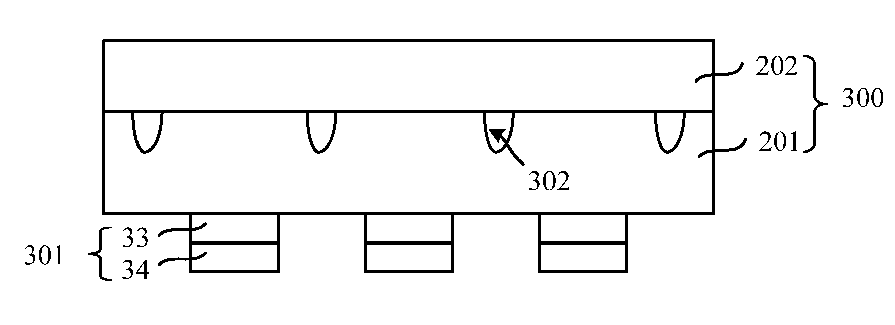
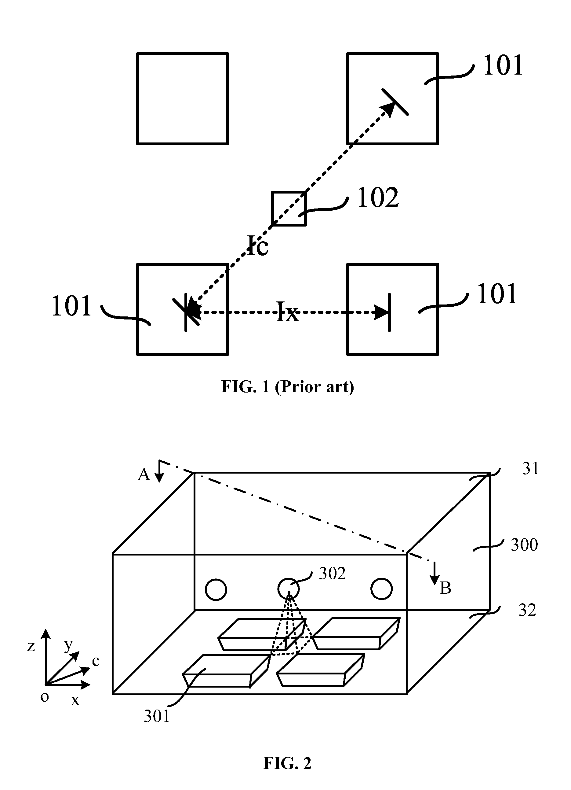
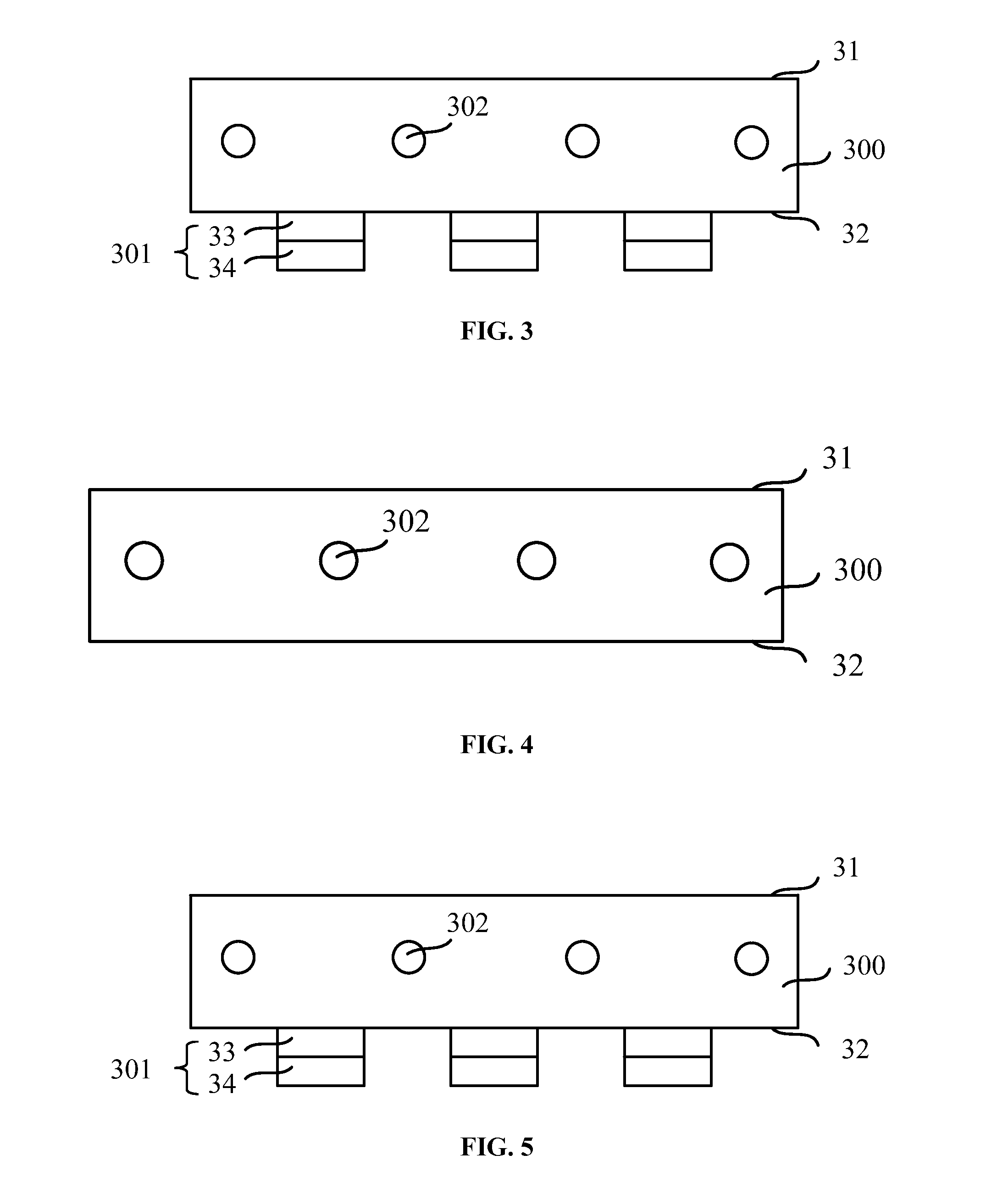
[0021]Referring to FIG. 1, the main patterns 101 and the assisting pattern 102 are on a same surface; and the assisting pattern 102 is between the main patterns 101. When the critical dimension of the main patterns 101 continuously decreases, distances between main patterns 101 may also continuously decrease, thus there may be no room to add assisting patterns 102. Thus, a layout of the main patterns 101 and the assisting pattern 102 be challenging. A routine resolve of the patterns in a photoresist layer may also be challenging. Thus, the process window of a photolithography process may be limited. A mask with three-dimensional scattering assisting patterns functioning as a refractive index disturbance is disclosed to overcome the...


PUM

PropertyMeasurementUnit
distanceaaaaaaaaaa
diameteraaaaaaaaaa
focus depthaaaaaaaaaa

Abstract

A photolithographic mask is provided. The photolithographic mask includes a substrate having a first surface configured as a light incidence plane of an exposure light and a second surface. The photolithographic mask also includes a plurality of scattering centers functioning as a refractive index disturbance inside the substrate. Further, the photolithographic mask includes a plurality of mask patterns on the second surface of the substrate.

Description

CROSS-REFERENCES TO RELATED APPLICATIONS[0001]This application claims the priority of Chinese patent application No. 201310315233.6, filed on Jul. 24, 2013, the entirety of which is incorporated herein by reference.FIELD OF THE INVENTION[0002]The present invention generally relates to the field of semiconductor manufacturing technology and, more particularly, relates to photolithographic masks and fabrication techniques thereof.BACKGROUND[0003]Photolithography is a major process in the manufacturing of integrated circuits (ICs). A major task of a photolithography process is to transfer patterns on a mask to a photoresist layer on a wafer. The projection light propagates through the patterns on the mask, and arrives at the wafer. The patterns on the mask are equivalent to obstacles in the propagation path of the projection light, thus the patterns on mask may be obtained on the wafer. According to the principle of light diffraction and the principle of light interference, a light dif...

Claims


Application Information

Patent Timeline
Patent Type & Authority Patents(United States)
IPC IPC(8): G03F1/38
CPCG03F1/38
Inventor CAI, BOXIU
Owner SEMICON MFG INT (SHANGHAI) CORP
Why Eureka
Try Eureka