Multi-layered chip electronic component

a technology of electronic components and layers, applied in the direction of stacked capacitors, fixed capacitor details, cores/yokes, etc., can solve the problems of reduced inductance due to dc in multi-layered chip type inductors, and achieve excellent dc bias characteristics and sufficient capacity

Inactive Publication Date: 2016-05-24
SAMSUNG ELECTRO MECHANICS CO LTD
View PDF14 Cites 0 Cited by
  • Summary
  • Abstract
  • Description
  • Claims
  • Application Information

AI Technical Summary

Benefits of technology

[0012]An aspect of the present invention provides a multi-layered chip component having excellent DC bias characteristics while implementing miniaturization and securing sufficient capacity, by adjusting a thickness of a non-magnetic layer to be thin.

Problems solved by technology

Recently, as multi-layered chip type inductors have been miniaturized, the multi-layered chip type inductors have had a defect of reduced inductance due to DC bias.

Method used


Image

  • Multi-layered chip electronic component
  • Multi-layered chip electronic component
  • Multi-layered chip electronic component

Examples


experimental example

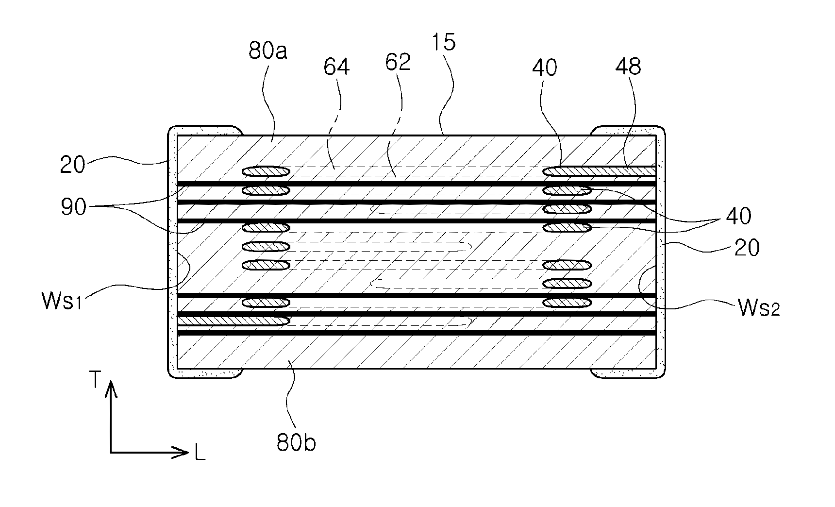
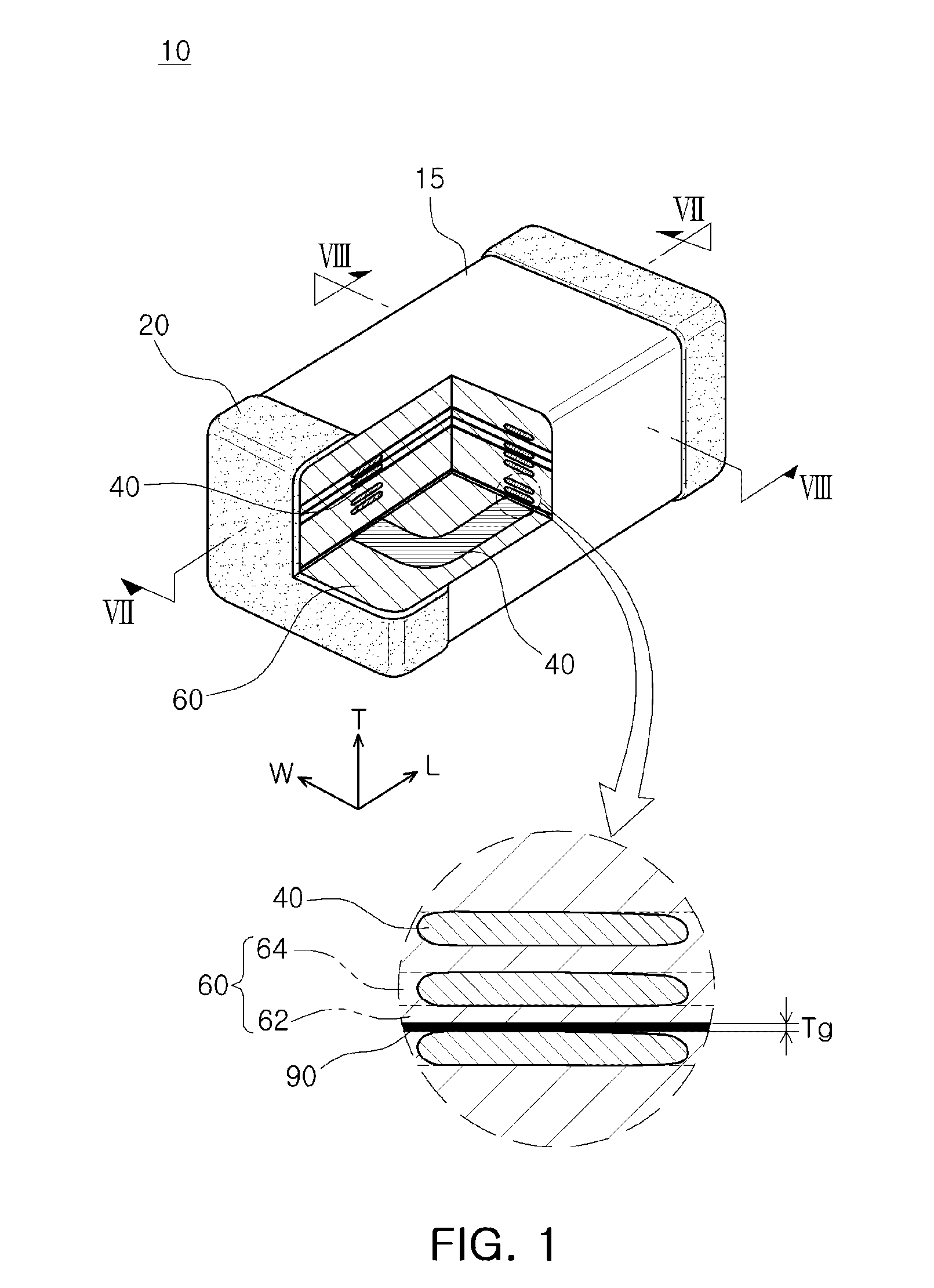
[0095]The multi-layered chip type inductor according to the Inventive Examples of the present invention and Comparative Examples was manufactured as follows. A plurality of magnetic green sheets, manufactured by applying a slurry including the Ni—Zu—Cu-based ferrite powder to a carrier film and drying the slurry were prepared.

[0096]Next, the conductive patterns are formed by applying a silver (Ag) conductive paste to the magnetic green sheet using a screen. In addition, the single multi-layered carrier is formed together with the magnetic green sheet by applying the ferrite slurry to the magnetic green sheet around the conductive pattern so as to be a common layer with the conductive pattern.

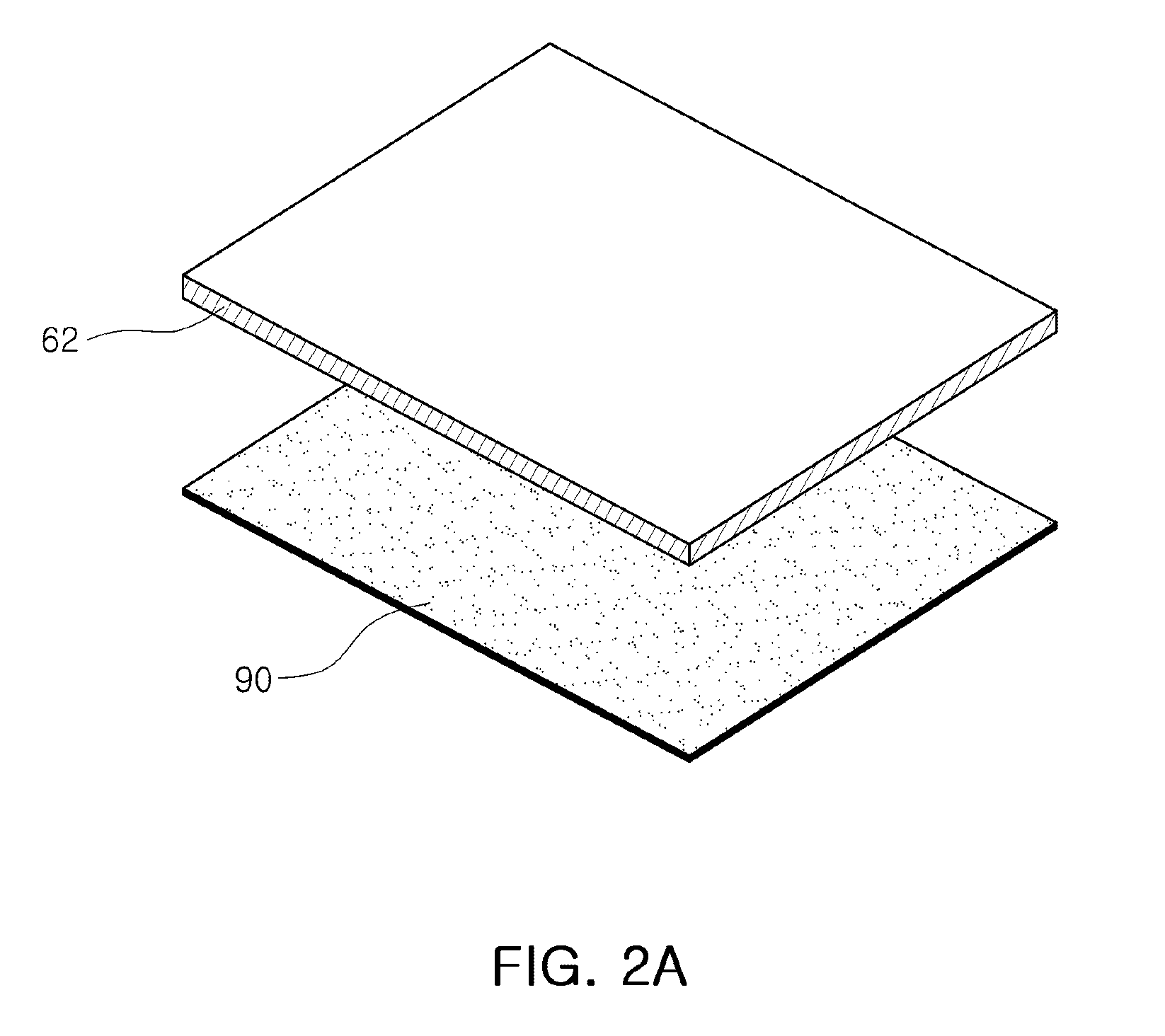
[0097]The stacked carriers in which the conductive patterns are formed are repeatedly multi-layered and the conductive patterns are electrically connected, thereby forming the coil pattern in the stacking direction. In addition, the non-magnetic gap layer may be formed between the conductor patt...


PUM

PropertyMeasurementUnit
widthaaaaaaaaaa
widthaaaaaaaaaa
thicknessaaaaaaaaaa

Abstract

There is provided a multi-layered chip electronic component including: a multi-layered body including a 2016-sized or less and a plurality of magnetic layers; conductive patterns electrically connected in a stacking direction to form coil patterns, within the multi-layered body; and non-magnetic gap layers formed over a laminated surface of the multi-layered body between the multi-layered magnetic layers and having a thickness Tg in a range of 1 μm≦Tg≦7 μm, wherein the number of non-magnetic gap layers may have the number of gap layers in a range between at least four layers among the magnetic layers and a turns amount of the coil pattern.

Description

CROSS-REFERENCE TO RELATED APPLICATIONS[0001]This application claims the priority of Korean Patent Application No. 10-2012-0063795 filed on Jun. 14, 2012, in the Korean Intellectual Property Office, the disclosure of which is incorporated herein by reference.BACKGROUND OF THE INVENTION[0002]1. Field of the Invention[0003]The present invention relates to a multi-layered chip electronic component.[0004]2. Description of the Related Art[0005]An inductor, a multi-layered chip component, is a representative passive element capable of removing noise by configuring an electronic circuit, together with a resistor and a capacitor.[0006]A multi-layered chip type inductor may be manufactured by printing and stacking conductive patterns so as to form a coil in a magnetic substance. The multi-layered chip type inductor has a structure in which a plurality of magnetic layers on which conductive patterns are formed are stacked. Internal conductive patterns within the multi-layered chip type induct...

Claims


Application Information

Patent Timeline
Patent Type & Authority Patents(United States)
IPC IPC(8): H01F5/00H01F3/14H01F27/28H01F17/00H01F27/29
CPCH01F3/14H01F17/0013H01F17/0033H01F27/292H01G4/12H01G4/30
Inventor HAHN, JIN WOOKIM, MYEONG GIAN, SUNG YONGKIM, IC SEOBMOON, BYEONG CHEOL
Owner SAMSUNG ELECTRO MECHANICS CO LTD
Why Eureka
Try Eureka