Dielectric composition, dielectric element, electronic component and laminated electronic component

a technology of dielectric elements and dielectric layers, applied in the direction of fixed capacitors, basic electric elements, electrical equipment, etc., can solve the problems of dielectric layer reduction, pd is costly, and the insulation resistance of the dielectric layer deteriorates markedly, and achieves a compact and higher performance

Active Publication Date: 2019-08-20
EPCOS AG
View PDF30 Cites 0 Cited by
  • Summary
  • Abstract
  • Description
  • Claims
  • Application Information

AI Technical Summary

Benefits of technology

[0014]Embodiments provide a dielectric composition which has excellent DC bias characteristics and high insulation resistance at high temperatures. Further embodiments provide a dielectric element, an electronic component and a laminated electronic component.
[0016]A dielectric composition having this constitution can achieve excellent DC bias characteristics and high insulation resistance at high temperatures.
[0019]The dielectric composition according to embodiments of the present invention preferably contains between 0.2 molar parts and 1 molar part of at least one from the group consisting of Cu, Mn, Zn, Mg and Co as an auxiliary component, with respect to 100 molar parts of Ti contained in the main component. As a result, the sintering properties are improved and it is possible to achieve high insulation resistance.
[0021]The dielectric element according to embodiments of the present invention comprises the abovementioned dielectric composition and can therefore be made more compact and higher performing.
[0024]The electronic component and the laminated electronic component according to embodiments the present invention are provided with a dielectric layer comprising the abovementioned dielectric composition and can therefore be made more compact and higher performing.

Problems solved by technology

There is a problem with a barium titanate-based dielectric composition, however, in that the insulation resistance thereof deteriorates markedly at high temperatures of 100° C. or above.
However, Pd is costly so in recent years use has also been made of relatively inexpensive base metals such as Ni and Cu.
When baking is carried out under a reducing atmosphere, however, the dielectric layer is reduced and there is a drop in insulation resistance.
However, although the dielectric constant of the dielectric composition in Patent Japanese Patent JP 3334607 is relatively high at around 900-950 when a DC electric field of 5 V / μm is applied, the dielectric constant decreases when an even higher DC electric field is applied, so the DC bias characteristics are inadequate to cope with the thinning of the layers which accompanies a reduction in size and increased capacity.

Method used


Image

  • Dielectric composition, dielectric element, electronic component and laminated electronic component

Examples


Embodiment Construction

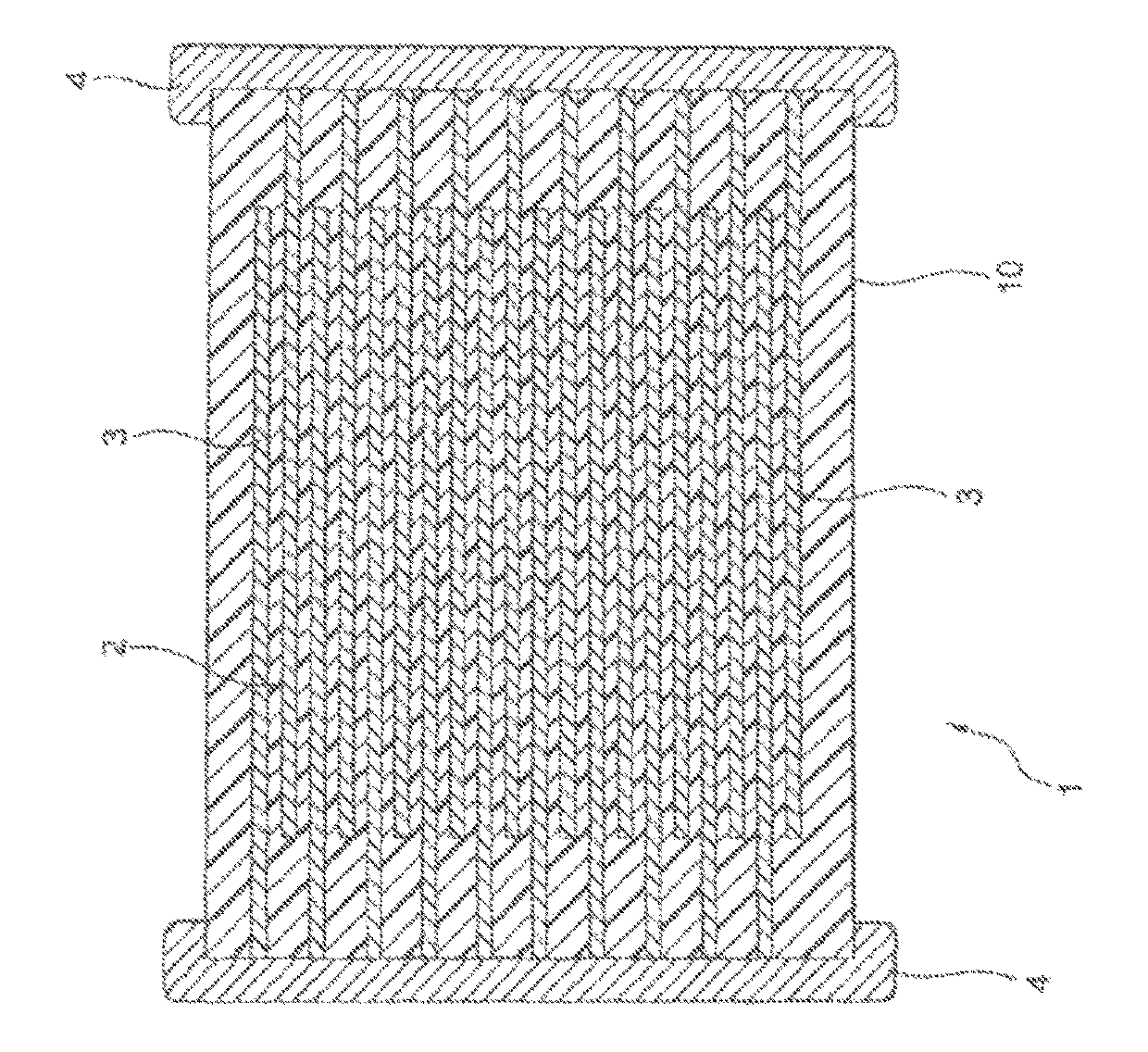
[0026]FIGURE shows a laminated ceramic capacitor 1 according to a mode of embodiment of the present invention comprising a capacitor element main body 10 having a structure in which dielectric layers 2 and internal electrode layers 3 are alternately stacked. The internal electrode layers 3 are stacked in such a way that the end surfaces thereof are alternately exposed at the two opposing ends of the capacitor element main body 10. A pair of external electrodes 4 is formed at both ends of the capacitor element main body 10, and are connected to the exposed end surfaces of the alternately-arranged internal electrode layers 3 to form a capacitor circuit.

[0027]Is shown in FIG. 1, a laminated ceramic capacitor 1 according to a mode of embodiment of the present invention comprises a capacitor element main body 10 having a structure in which dielectric layers 2 and internal electrode layers 3 are alternately stacked. The internal electrode layers 3 are stacked in such a way that the end su...


PUM

PropertyMeasurementUnit
grain sizeaaaaaaaaaa
insulation resistivityaaaaaaaaaa

Abstract

A dielectric composition, a dielectric element, an electronic component and a laminated electronic component are disclosed. In an embodiment the dielectric composition includes a perovskite compound comprising a main component having Bi, Na, Sr, Ln and Ti, wherein Ln is at least one type of a rare earth element, and wherein a mean crystal grain size is between 0.1 μm and 1 μm.

Description

[0001]This patent application is a national phase filing under section 371 of PCT / EP2016 / 061701, filed May 24, 2016, which claims the priority of Japanese patent application 2015-107731, filed May 27, 2015 and Japanese patent application 2015-256458, filed Dec. 28, 2015, each of which is incorporated herein by reference in its entirety.TECHNICAL FIELD[0002]The present invention relates to a dielectric composition, a dielectric element, an electronic component and a laminated electronic component which are advantageously used for medium- and high-voltage applications with a high rated voltage, and are also advantageously used under a high-temperature environment.BACKGROUND[0003]Laminated electronic components such as laminated ceramic capacitors are widely used as compact, large-capacity and highly reliable electronic components. As devices have become more compact and higher performing in recent years, there has been an increasingly strong demand for further miniaturization, increas...

Claims


Application Information

Patent Timeline
Patent Type & Authority Patents(United States)
IPC IPC(8): C04B35/475H01G4/12H01G4/228C04B35/64C04B35/626C04B35/47C04B35/462H01G4/30C04B41/88C04B41/51C04B35/638C04B41/45C04B41/00
CPCH01G4/1227C04B35/47C04B35/475C04B35/62685C04B35/638C04B35/64C04B41/009C04B41/4578C04B41/5111C04B41/88H01G4/1218H01G4/228H01G4/30C04B35/462C04B2235/785C04B2235/3201C04B2235/3203C04B2235/3206C04B2235/3213C04B2235/3224C04B2235/3225C04B2235/3227C04B2235/3236C04B2235/3262C04B2235/3277C04B2235/3281C04B2235/3284C04B2235/3298C04B2235/5445C04B2235/602C04B2235/612C04B2235/656C04B2235/6582C04B2235/768
Inventor IMURA, TOMOYATERADA, TOMOHIRO
Owner EPCOS AG
Why Eureka
Try Eureka