Singulation method for semiconductor package with plating on side of connectors

a technology of semiconductor packages and connectors, applied in semiconductor devices, semiconductor/solid-state device details, electrical devices, etc., can solve the problems of contaminated surface and undesirable oxide on the surface, and achieve the effect of preventing contamination of lead surfaces

Active Publication Date: 2016-05-24
UTAC HEADQUARTERS PTE LTD
View PDF53 Cites 3 Cited by
  • Summary
  • Abstract
  • Description
  • Claims
  • Application Information

AI Technical Summary

Benefits of technology

[0004]The present invention provides a new, useful, and non-obvious method of singulating and plating semiconductor packages, employing plating of the side surfaces of the leads of the leadframe in order to prevent contamination of the lead surfaces.

Problems solved by technology

As a result of the side surfaces 120b of the leads not being plated, their exposed surface, typically copper, is easy to react with oxygen, thereby resulting in undesirable oxide on the surface of the leads.
The contaminated surface will create problems when the semiconductor package 100 is soldered into a printed circuit board.

Method used


Image

  • Singulation method for semiconductor package with plating on side of connectors
  • Singulation method for semiconductor package with plating on side of connectors
  • Singulation method for semiconductor package with plating on side of connectors

Examples


Embodiment Construction

[0036]The following description is presented to enable one of ordinary skill in the art to make and use the invention and is provided in the context of a patent application and its requirements. Various modifications to the described embodiments will be readily apparent to those skilled in the art and the generic principles herein may be applied to other embodiments. Thus, the present invention is not intended to be limited to the embodiment shown but is to be accorded the widest scope consistent with the principles and features described herein.

[0037]This disclosure provides several embodiments of the present invention. It is contemplated that any features from any embodiment can be combined with any features from any other embodiment. In this fashion, hybrid configurations of the disclosed embodiments are well within the scope of the present invention.

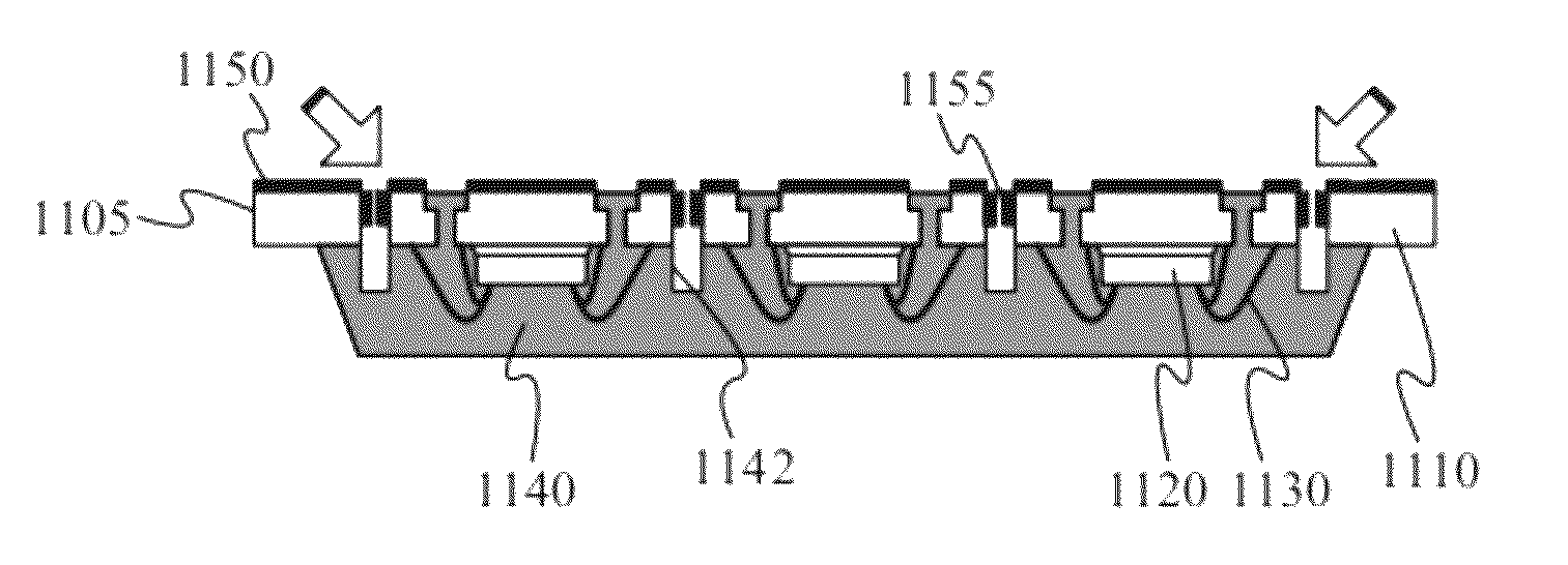
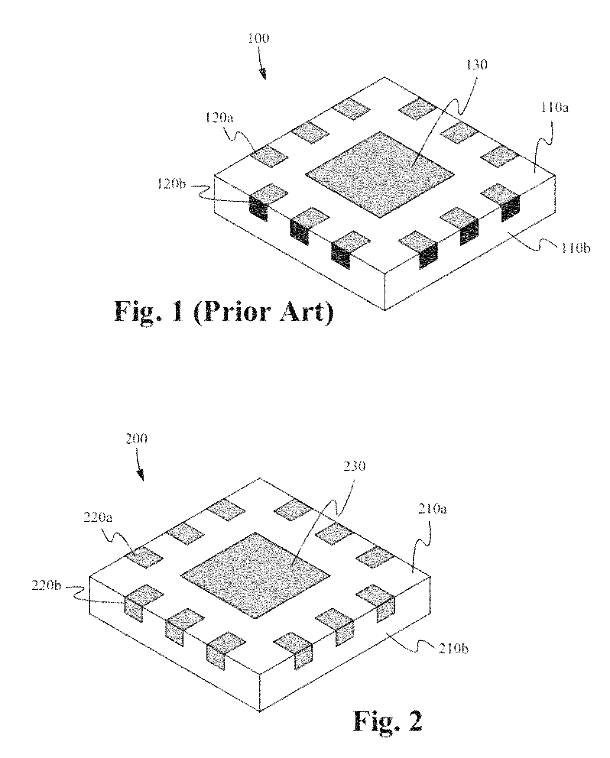
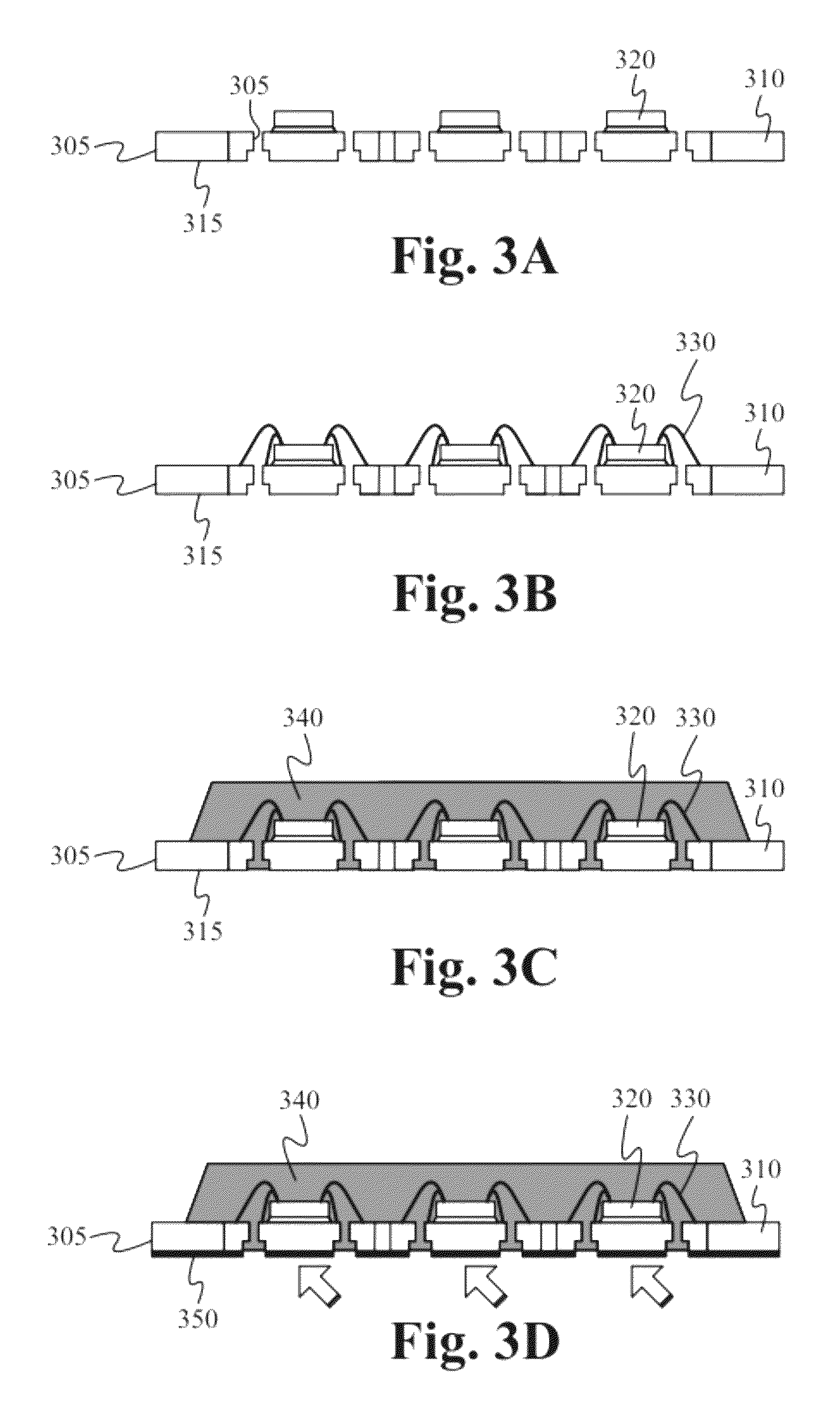
[0038]The present invention provides a new, useful, and non-obvious method of singulating and plating semiconductor packages, emplo...


PUM


Abstract

A method of singulating semiconductor packages, the method comprising: providing a plurality of semiconductor dies coupled to a single common leadframe, wherein a molding compound at least partially encases the semiconductor dies and the leadframe; singulating the plurality of semiconductor dies, wherein the leadframe is at least partially cut between adjacent semiconductor dies, thereby forming exposed side surfaces on leads of the leadframe; and plating the exposed side surfaces of the leads with a plating material, wherein the plating material is a different material than the leads. In some embodiments, singulating the plurality of semiconductor dies comprises performing a full cut of the leadframe. In some embodiments, singulating the plurality of semiconductor dies comprises performing separate partial cuts of the leadframe.

Description

CROSS-REFERENCE TO RELATED APPLICATIONS[0001]This application claims priority to U.S. Provisional Application Ser. No. 61 / 378,776, filed Aug. 31, 2010, entitled “SINGULATION METHOD FOR SEMICONDUCTOR PACKAGE WITH PLATING ON SIDE OF CONNECTORS” and to U.S. Provisional Application Ser. No. 61 / 412,183, filed Nov. 10, 2010, entitled “SINGULATION AND PLATING METHOD FOR SEMICONDUCTOR PACKAGE,” both of which are hereby incorporated by reference in their entirety as if set forth herein.FIELD OF THE INVENTION[0002]The present invention relates to the field of semiconductor packages. More specifically, the present invention relates to a singulation and plating method for semiconductor packages.BACKGROUND OF THE INVENTION[0003]FIG. 1 is a perspective view of a prior art semiconductor package 100 having a top surface 110a and side surfaces 110b formed by a molding compound. A leadframe is encased in the molding compound, with the top surfaces 120a and side surfaces 120b of its leads being expose...

Claims


Application Information

Patent Timeline
Patent Type & Authority Patents(United States)
IPC IPC(8): H01L21/78H01L21/56H01L23/495H01L23/00
CPCH01L23/49582H01L21/561H01L24/97H01L23/49548H01L24/45H01L24/48H01L24/73H01L2221/68331H01L2224/32245H01L2224/45124H01L2224/45144H01L2224/45147H01L2224/48091H01L2224/48247H01L2224/48257H01L2224/73265H01L2224/83192H01L2224/92247H01L2224/97H01L2924/014H01L2924/01005H01L2924/01013H01L2924/01028H01L2924/01029H01L2924/01033H01L2924/01047H01L2924/01079H01L2924/01082H01L2924/15313H01L2924/181H01L2224/85H01L2224/83H01L2924/00014H01L2924/00012H01L2924/00H01L2924/18301H01L21/288H01L21/4842H01L21/565H01L21/78H01L23/3107H01L23/49541H01L24/32H01L24/49H01L24/83H01L24/85H01L24/92H01L2224/48106H01L2924/01046H01L2924/0105H01L2924/0132H01L2924/0133H01L2924/17747H01L2924/1815
Inventor SIRINORAKUL, SARAVUTHNONDHASITTHICHAI, SOMCHAI
Owner UTAC HEADQUARTERS PTE LTD
Why Eureka
Try Eureka