

Method for fabricating multi-gate structure device with source and drain having quasi-SOI structure
- Summary
- Abstract
- Description
- Claims
- Application Information
AI Technical Summary
Benefits of technology
Problems solved by technology
Method used
Image

Examples
Embodiment Construction
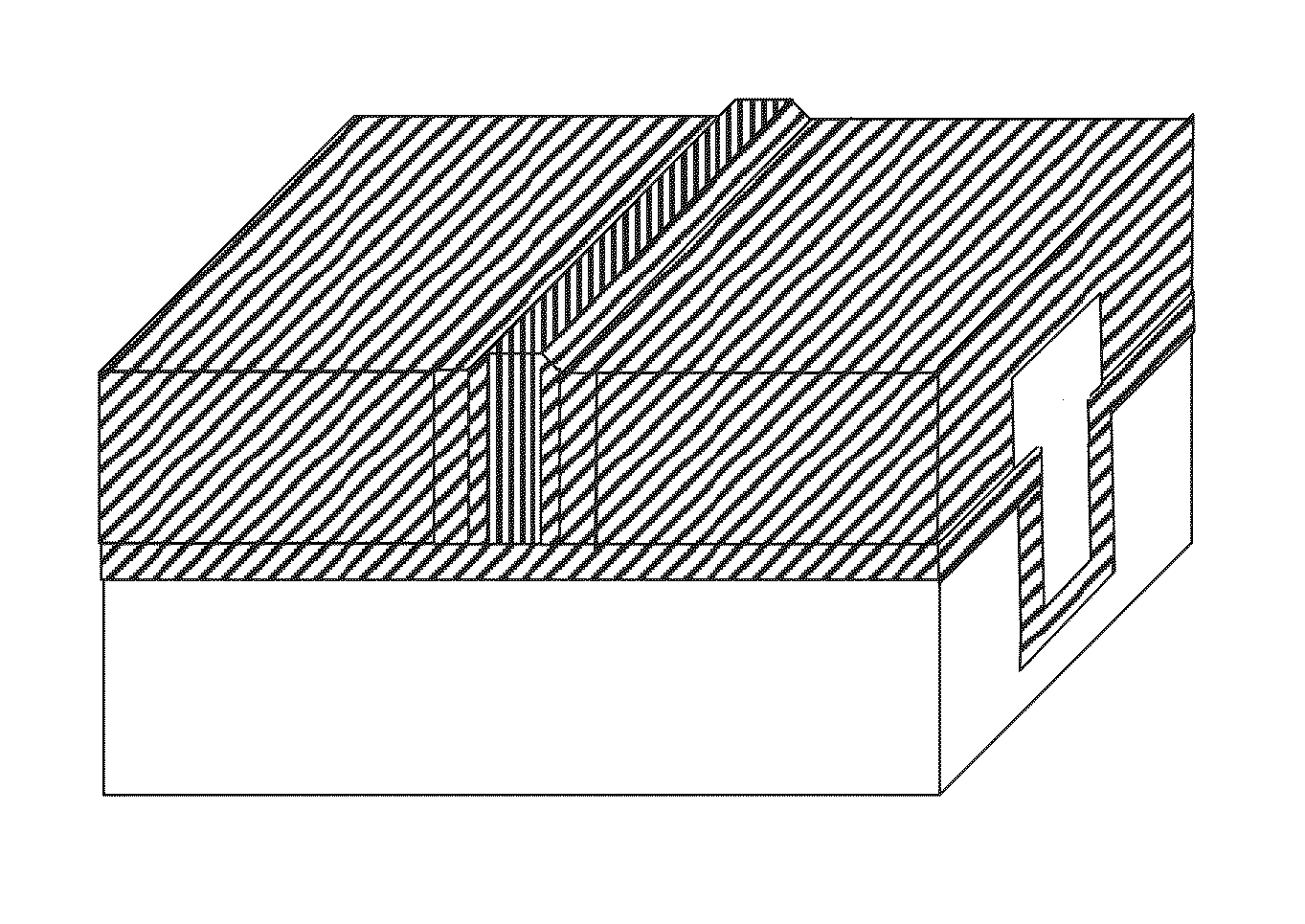
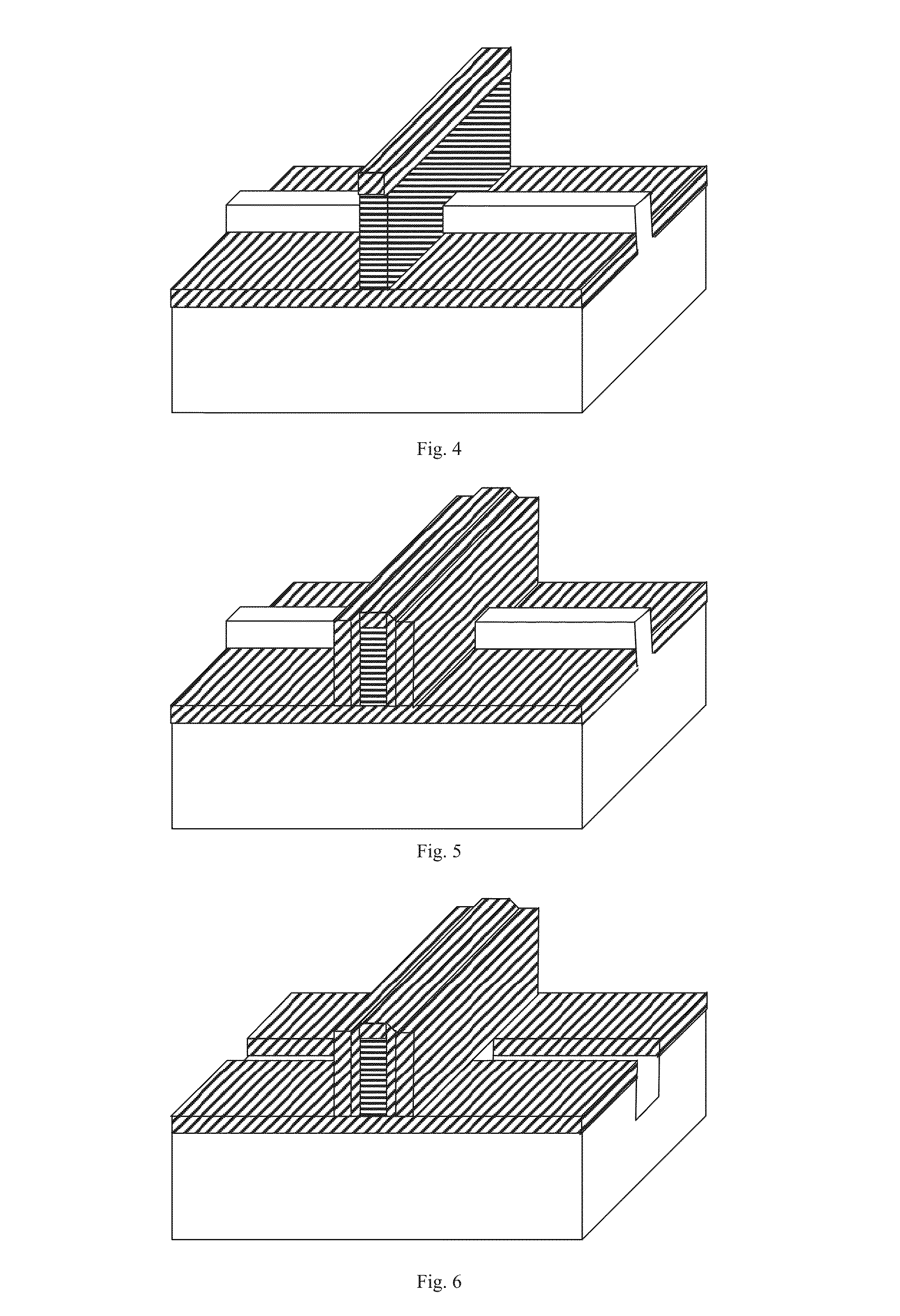
[0077]Hereinafter, the present invention will be described in detail in conjunction with specific embodiments. A process for fabricating a multi-gate structure device with an ultra short channel according to the present invention will be given. The process will be described by example of a tri-gate structure device, which does not limit the scope of the present invention in any way.
[0078]An n-type tri-gate field effect transistor, which has a fin bar with a width of 10 nm, a height of 30 nm and a channel length of 25 nm, is fabricated according to the following steps.
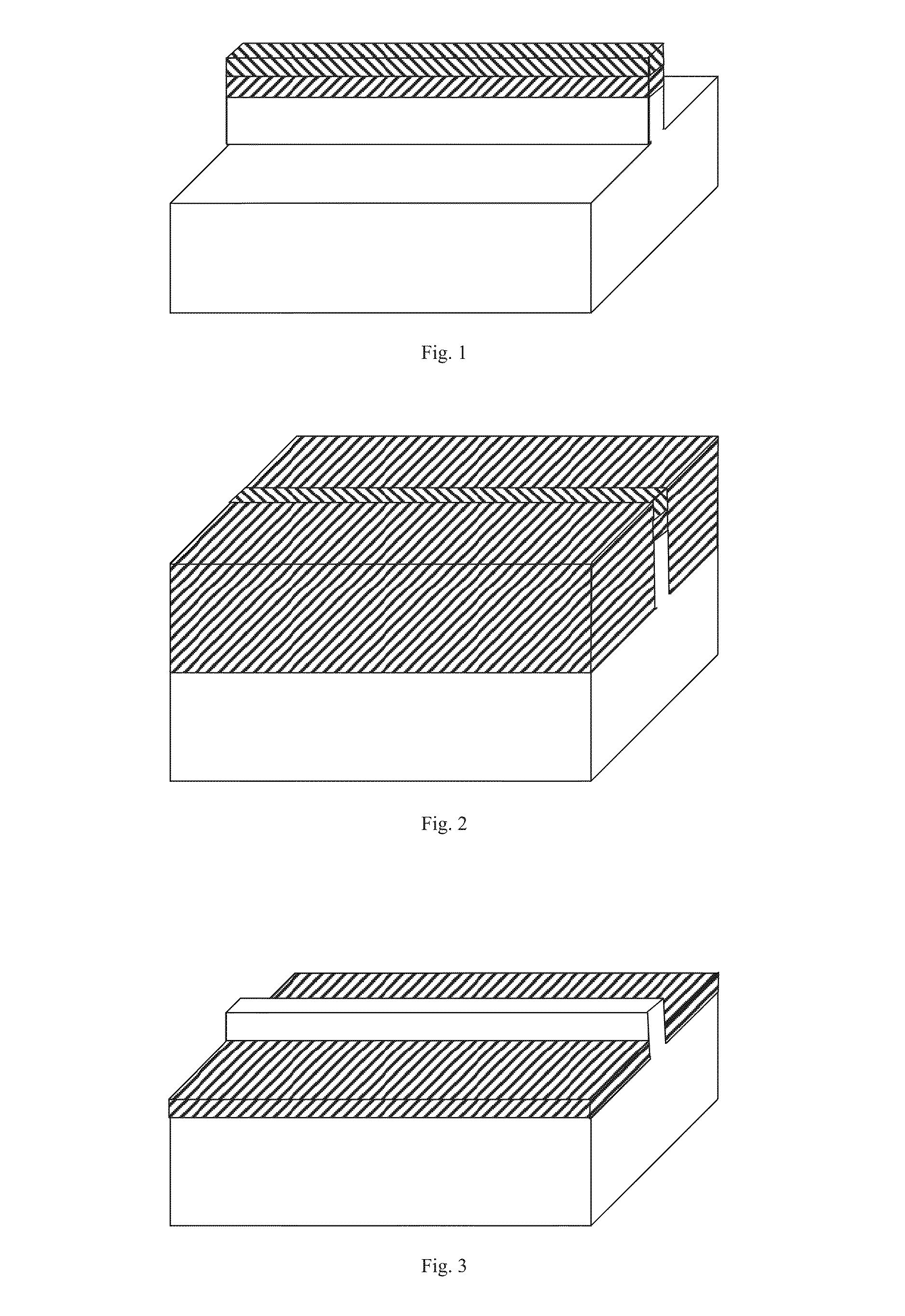
[0079]1. A silicon oxide layer of 200 Å is deposited on a silicon substrate through a low pressure chemical vapor deposition process.
[0080]2. A silicon nitride layer of 500 Å is deposited on the silicon oxide layer through a low pressure chemical vapor deposition process.
[0081]3. A fin bar with a width of 20 nm is defined through a photolithography process.
[0082]4. The silicon nitride layer of 500 Å is subjected to an a...
PUM
 Abstract
Description
Claims
Application Information