Eureka AIR delivers breakthrough ideas for toughest innovation challenges, trusted by R&D personnel around the world.

Fault detection system, generation circuit, and program

a fault detection and generation circuit technology, applied in error detection/correction, instruments, transportation and packaging, etc., can solve the problems of scan flip-flops acquiring and holding an erroneous test response value, increasing power consumption, and reducing the shift power in the scan-out operation. , to achieve the effect of maintaining the fault coverage, and reducing the shift power in the scan-out operation

Active Publication Date: 2016-07-05
PRIMETALS TECH GERMANY +1
View PDF8 Cites 0 Cited by
  • Summary
  • Abstract
  • Description
  • Claims
  • Application Information

AI Technical Summary

Benefits of technology

[0021]With the aforementioned aspects of the present invention, such an arrangement is capable of giving a new logic value to the output logic value (test output) captured finally by the FFs in the capture mode before performing fault detection. Thus, by appropriately selecting the FFs to be supplied with a new logic value and by appropriately selecting such a new logic value, such an arrangement provides a reduction in shift power in the scan-out operation while maintaining the fault coverage.
[0022]With an ordinary scan test, it is inconceivable that the test output signal output from the logic circuit to be subjected to the fault detection would be changed before the fault detection. The originality of the present invention is that the logic value of each selected FF is changed before the fault detection so as to reduce the shift power in the scan-out operation, based on the findings that the fault coverage can be maintained even if the logic values of the FFs that satisfy a predetermined condition are changed before the captured logic values are shifted out.
[0023]With the second aspect of the present invention, fault detection is performed multiple times in the same capture mode for the FFs connected to the acquisition circuit. Thus, there is no need to again shift out the logic values captured finally in the capture mode by such FFs connected to the acquisition circuit in the final stage. Thus, by supplying a new logic value to each of the FFs connected to the acquisition circuit, such an arrangement allows the shift power to be reduced more easily while maintaining the fault coverage.
[0024]With the third aspect of the present invention, such an arrangement provides an advantage of a marked reduction in the shift power.
[0025]With the fourth aspect of the present invention, by supplying a new logic value to the FFs that have each captured the same logic value in the final two captures, such an arrangement allows the shift power to be reduced. As described later regarding the experiment results obtained by the present inventors, this is because, when the same logic value is captured from a given FF in the final two captures, there is a high probability that such a FF does not contribute to improving the transition delay fault coverage. Thus, such an arrangement allows the shift power to be reduced more easily while maintaining the transition delay fault coverage.
[0026]With the fifth aspect of the present invention, such an arrangement is capable of supplying a logic value that has a high probability of reducing the shift power.

Problems solved by technology

In a scan test, an increase in power consumption leads to IR drop, a temporary drop in the power supply voltage.
In some cases, this leads to a malfunction of a logic circuit, resulting in a scan flip-flop acquiring and holding an erroneous test response value.
This leads to the occurrence of error in a test, in which a given logic circuit is judged to be defective even if it operates normally in a normal operation.
As a result, such a test leads to yield loss.
In particular, in a case in which a semiconductor logic circuit is configured with a very fine size on a very large scale and configured to operate with a low power supply voltage, such test error leads to a marked yield loss.
Furthermore, the shift power is classified into two kinds, i.e., power consumption required for a scan-in operation and power consumption required for a scan-out operation.

Method used


Image

  • Fault detection system, generation circuit, and program
  • Fault detection system, generation circuit, and program
  • Fault detection system, generation circuit, and program

Examples


example 1

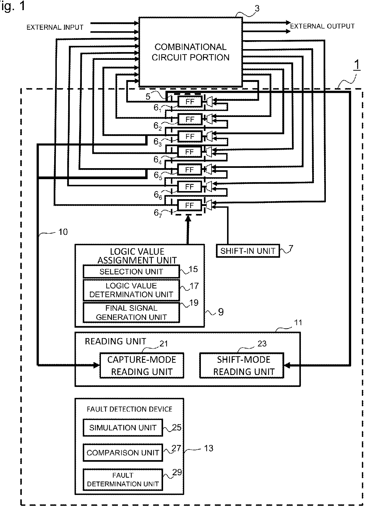
[0037]FIG. 1 is a block diagram showing a schematic configuration of a fault detection system 1 according to the example of the present invention. Description will be made below regarding the schematic configuration of the fault detection system 1 shown in FIG. 1.

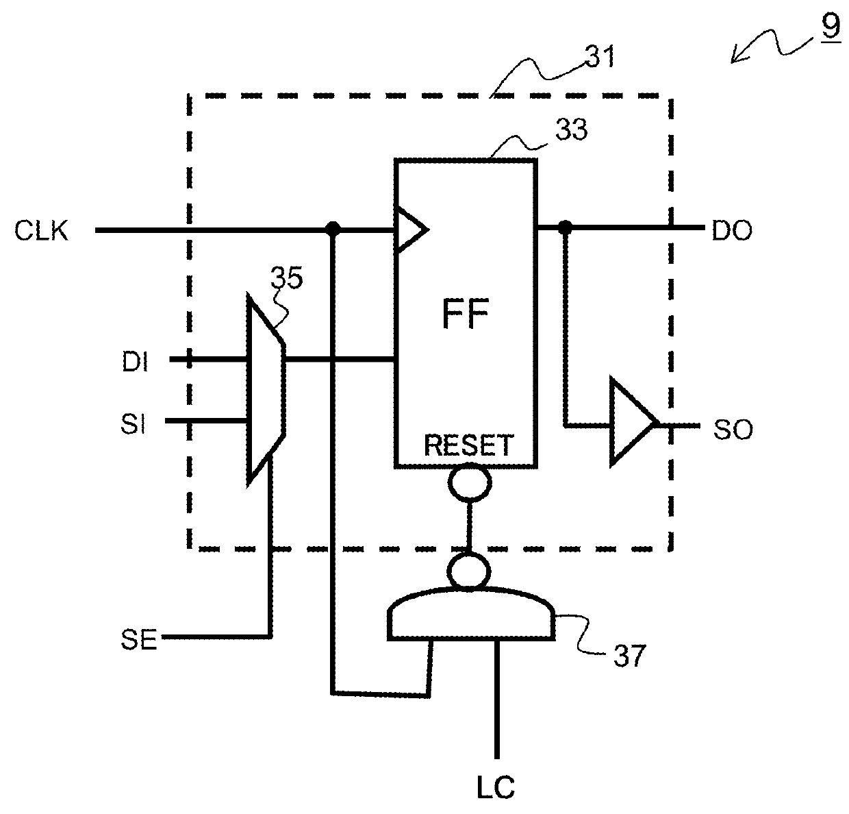
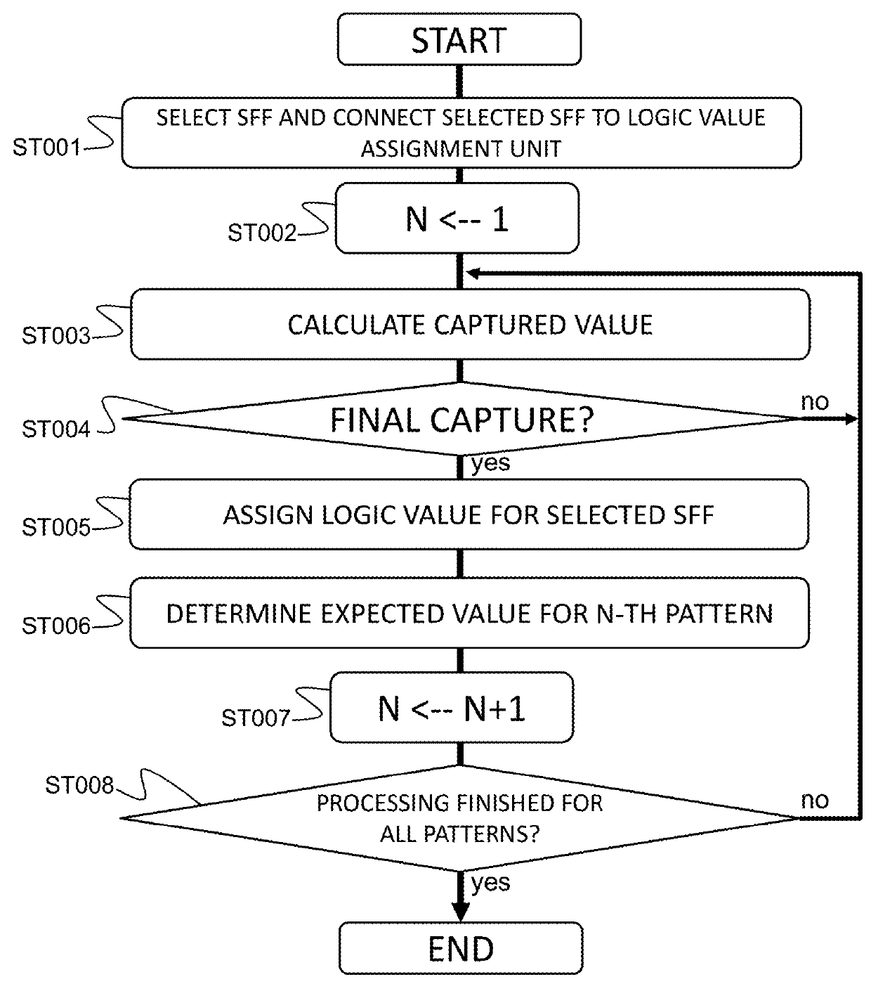
[0038]The fault detection system 1 (an example of a “fault detection system” in the claims) is configured to detect a fault that occurs in a combinational circuit portion 3 (an example of a “logic circuit” in the claims) by means of a scan test. The fault detection system 1 includes a storage circuit portion 5 that captures a logic value output from the combinational circuit portion 3, a shift-in unit 7 that shifts a logic value into the storage circuit portion 5, a logic value assignment unit 9 (an example of “assignment unit” in the claims) that assigns a logic value for the storage circuit portion 5 after the final capture, a reading unit 11 that reads out the logic value stored in the storage circuit portion 5, and a fa...

example 2

[0058]Description will be made regarding multiple example circuit configurations configured to supply a SFF with a logic value as a specified value. Description will be made in the present example regarding an example circuit configuration employing a multiplexer.

[0059]Referring to FIG. 4, a SFF 39, which is selected by the selection unit, is connected to the output stream of a multiplexer 41 configured such that the output signal line from the combinational circuit portion 3 and a signal line that supplies a logic value of 0 are each connected as its input stream, and the final signal is used as a selection control input signal.

[0060]In the capture mode, when a signal value of 0 is set for the final signal line, the multiplexer 41 supplies the DI signal value to the SFF 39. When a signal value of 1 is set for the final signal line, which means the final capture, a logic value of 0 is supplied to the SFF 39.

[0061]It should be noted that a logic value of 1 may be supplied to the SFF ...

example 3

[0062]Next, description will be made regarding a circuit configuration configured to supply a given SFF with the same logic value as an adjacent SFF arranged in the scan chain. In FIG. 5, the output line of a NAND gate 47 is connected to the set terminal (SET) of a selected SFF 43 in a low-active state. The NAND gate 47 uses the capture output signal line of an adjacent SFF 45, the final signal line, and the clock signal line as its inputs. Furthermore, the output line of the NAND gate 49 is connected to the reset terminal of the SFF 43 in a low-active state. The NAND gate 49 uses, the inverted value of the capture output signal line of the adjacent SFF 45, the final signal line, and the clock signal line as its input.

[0063]When the final signal is supplied in the capture mode, and when the adjacent SFF 45 captures a logic value of 1, the SFF 43 receives a set input of 0 and a reset input of 1. In this case, low-active set is activated, and accordingly, the SFF 43 outputs 1. On the ...


PUM


Abstract

The purpose of the invention is to provide a fault detection system etc., that reduces shift power in scan-out while maintaining the fault coverage. The fault detection system configured to detect a fault in a logic circuit by means of a scan test, includes: multiple flip-flops; a final signal generation unit that generates a final signal indicating a final capture in a capture mode; an assignment unit that differs from the logic circuit and the flip-flops, and that sets a logic signal for a part of the flip-flops upon receiving the final signal; and a fault detection device that detects a fault by making a comparison between a test output captured from the logic circuit and including the logic value set by the assignment unit and a test output to be obtained when the logic circuit has no fault and including the logic value set by the assignment unit.

Description

TECHNICAL FIELD[0001]The present invention relates to a fault detection system, a generation circuit, and a program, and particularly relates to a fault detection system and the like that detects a fault that occurs in a logic circuit by means of a scan test.BACKGROUND ART[0002]In a scan test, an increase in power consumption leads to IR drop, a temporary drop in the power supply voltage. In some cases, this leads to a malfunction of a logic circuit, resulting in a scan flip-flop acquiring and holding an erroneous test response value. This leads to the occurrence of error in a test, in which a given logic circuit is judged to be defective even if it operates normally in a normal operation. As a result, such a test leads to yield loss. In particular, in a case in which a semiconductor logic circuit is configured with a very fine size on a very large scale and configured to operate with a low power supply voltage, such test error leads to a marked yield loss. Thus, it is important to ...

Claims


Application Information

Patent Timeline
Patent Type & Authority Patents(United States)
IPC IPC(8): G06F11/00G01R31/3185G01R31/317G01R31/3177
CPCG01R31/31721G01R31/3177G01R31/318541G01R31/318575G01R31/28H01L21/822H01L27/04Y02T10/70
Inventor SATO, YASUOWANG, SENLINGMIYASE, KOHEIKAJIHARA, SEIJI
Owner PRIMETALS TECH GERMANY
Why Eureka
Eureka Blog
Learn More