
Semiconductor devices

a technology of semiconductor devices and semiconductors, applied in the direction of semiconductor devices, transistors, electrical equipment, etc., can solve the problems of disadvantageous formation of a number of transistors in a narrow horizontal area, and achieve the effects of reducing the separation distance between the gate patterns, reducing the defect of the extruded portions, and reducing the defect of the bridg

Active Publication Date: 2016-08-02
SAMSUNG ELECTRONICS CO LTD
View PDF18 Cites 5 Cited by
  • Summary
  • Abstract
  • Description
  • Claims
  • Application Information

AI Technical Summary

Benefits of technology

[0027]Thus, a sufficient distance between neighboring extruded portions may be maintained even though the separated distance between the gate patterns may be decreased. Accordingly, the gate patterns may be easily formed by a photolithography process, and bridge defects of the extruded portions may be decreased. In addition, transistors may be formed in a narrow horizontal area, and a high integrated semiconductor device may be accomplished.

Problems solved by technology

However, the formation of a number of transistors in a narrow horizontal area may be disadvantageous.

Method used


Image

  • Semiconductor devices
  • Semiconductor devices
  • Semiconductor devices

Examples


first embodiment

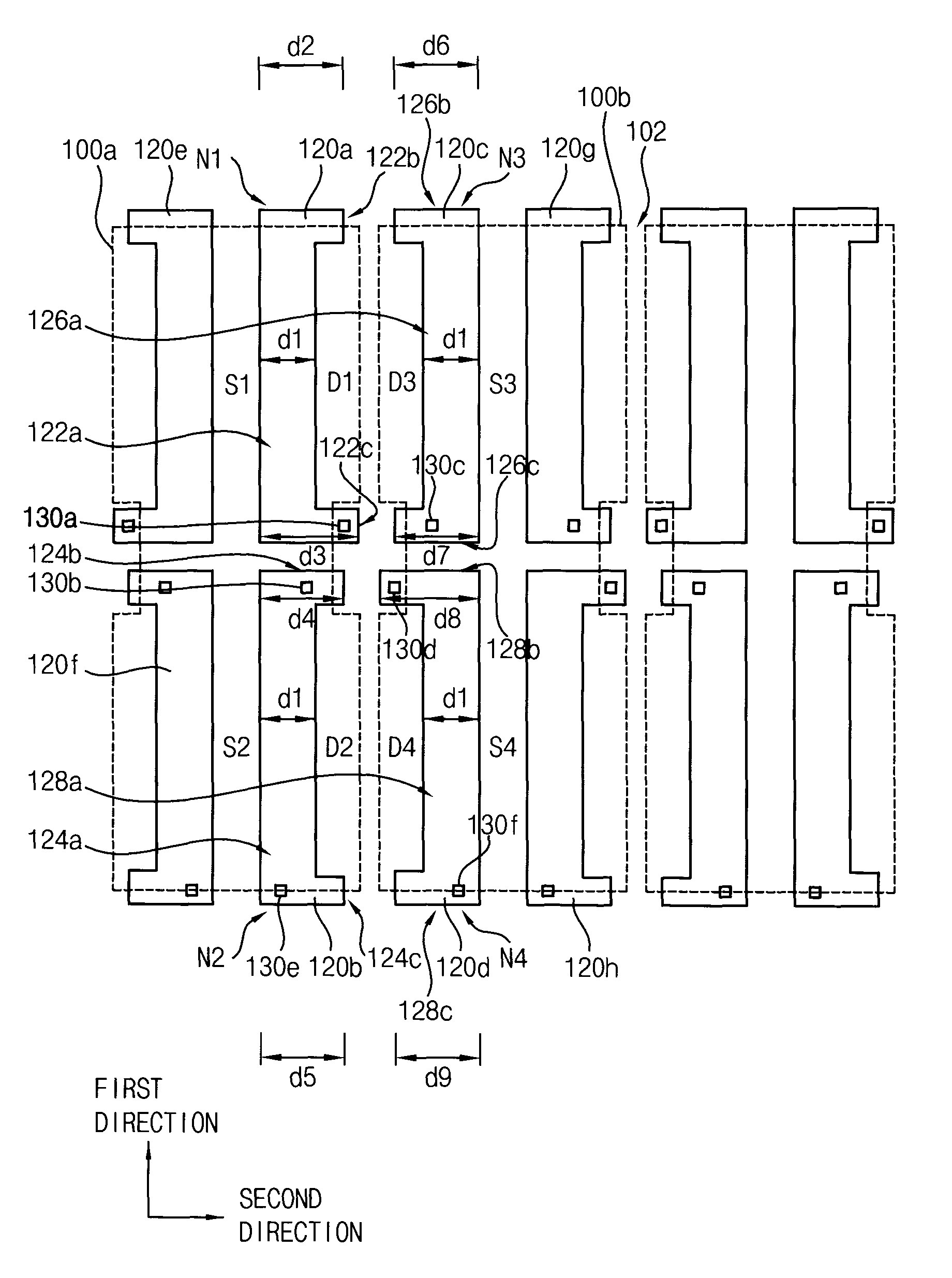
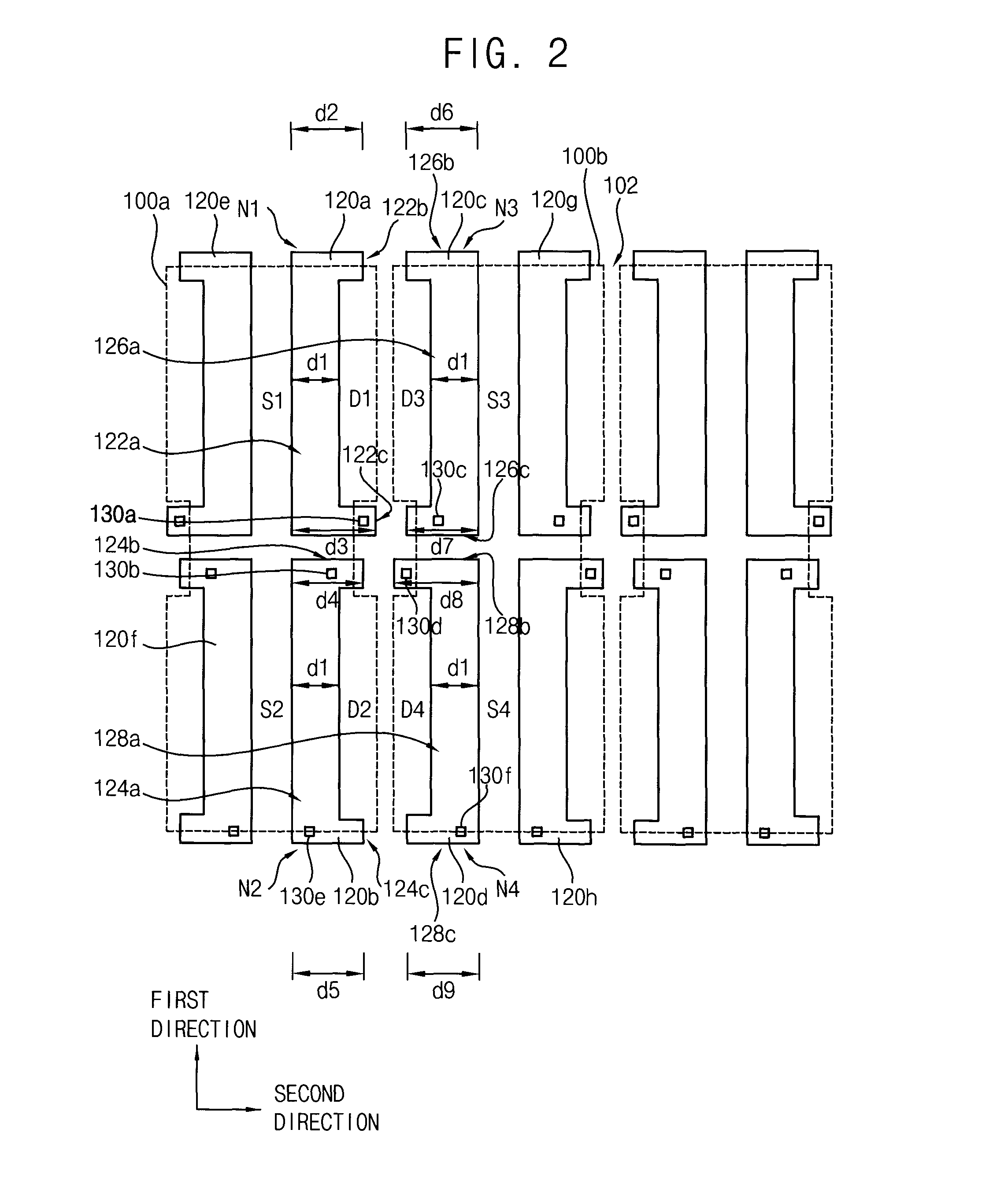
[0048]Example embodiments relate to a semiconductor device including a plurality of transistors repeatedly disposed with a certain gap. Examples of the semiconductor devices having the structure may include a sense amplifier. Thus, example embodiments may be explained referring to the sense amplifier hereinafter.

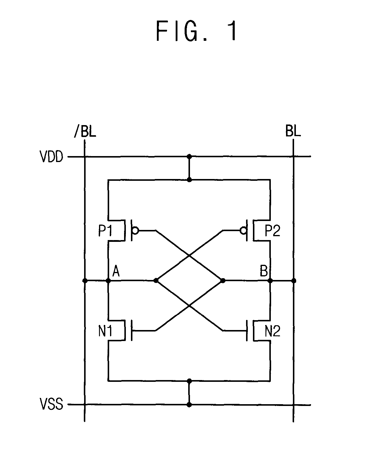
[0049]FIG. 1 is a circuit diagram of a unit sense amplifier of a semiconductor memory device according to an example embodiment.

[0050]Referring to FIG. 1, the unit sense amplifier of a semiconductor memory device may include two NMOS transistors N1 and N2, and two PMOS transistors P1 and P2, and may amplify data voltage. That is, the unit sense amplifier may include first and second NMOS transistors N1 and N2, and first and second PMOS transistors P1 and P2. The first PMOS transistor P1 and the first NMOS transistor N1 may be connected in series between power supply voltage and ground connection. In addition, the second PMOS transistor P2 and the second NMOS transistor N2 ma...

second embodiment

[0099]FIG. 4 is a layout of a portion of gate patterns included in a sense amplifier on a substrate in accordance with another example embodiment. FIG. 5 illustrates wirings formed on the gate patterns in FIG. 4.

[0100]In order to explain the layout in accordance with example embodiments, only the NMOS transistors formed in the first region of the substrate may be illustrated in FIG. 4.

[0101]Referring to FIG. 4, first and second active regions 100a and 100b for forming NMOS transistors may be provided in the substrate. Between the first and second active regions 100a and 100b, a device isolation region may be provided. The first and second active regions 100a and 100b may be the same as the explanation referring to FIG. 2.

[0102]On the first active region 100a, first and second gate patterns 120a and 120b may be provided. On the second active regions 100b, third and fourth gate patterns 120c and 120d may be provided. The first to fourth gate patterns 120a to 120d may be the same as th...

third embodiment

[0112]FIG. 6 is a layout of a portion of gate patterns included in a sense amplifier on a substrate in accordance with still another example embodiment. FIG. 7 illustrates wirings formed on the gate patterns in FIG. 6.

[0113]In order to explain the layout in accordance with example embodiments, only the NMOS transistors formed in the first region of the substrate may be illustrated in FIG. 6.

[0114]Referring to FIG. 6, first and second active regions 200a and 200b for forming NMOS transistors may be provided in the substrate. The first and second active regions 200a and 200b may have isolated shapes extended lengthily in the first direction. The first and second active regions 200a and 200b may have different shapes from each other. The first and second active regions 200a and 200b may be alternately and repeatedly disposed in the second direction. Between the first and second active regions 200a and 200b, a device isolation region may be provided.

[0115]The first active region 200a ma...


PUM


Abstract

Semiconductor devices include a first gate pattern provided on the first active region, a second gate pattern over the first active region, a third gate pattern over the second active region, and a fourth gate pattern over the second active region. The second gate pattern is parallel to the first gate pattern in a first direction. The third gate pattern has an asymmetric shape to the first gate pattern with respect to the first direction, and the fourth gate pattern is parallel to the third gate pattern in the first direction, and has an asymmetric shape to the second gate pattern with respect to the first direction. MOS transistors having good properties may be provided in a narrow horizontal area. The MOS transistors may be used in highly stacked semiconductor devices.

Description

CROSS-REFERENCE TO RELATED APPLICATION[0001]This application claims priority the benefit of priority under 35 USC §119 to Korean Patent Application No. 10-2013-0007222 filed on Jan. 23, 2013 in the Korean Intellectual Property Office (KIPO), the entire disclosure of which is incorporated herein by reference.BACKGROUND[0002]1. Field[0003]Example embodiments relate to semiconductor devices. More particularly, example embodiments relate to semiconductor devices including transistors and / or methods of manufacturing the same.[0004]2. Description of the Related Art[0005]The sense amplifier of a semiconductor memory device may include a pull up device using a PMOS transistor and a pull down device using an NMOS transistor, and may amplify and output the data voltage of a bit line and a bit line bar. Recently, as the cell size of a semiconductor memory device decreases, a horizontal area occupied by the sense amplifier may be largely decreased. However, the formation of a number of transist...

Claims


Application Information

Patent Timeline
Patent Type & Authority Patents(United States)
IPC IPC(8): H01L27/02H01L27/11H01L27/118
CPCH01L27/1104H01L27/0207H01L2027/11812H01L2027/11838H10B10/12H01L27/02
Inventor SONG, HYUN-SEUNGKIM, KYUNG-EUNPARK, JAE-KYUN
Owner SAMSUNG ELECTRONICS CO LTD
Learn More