Semiconductor storage device and system provided with same
a memory device and memory technology, applied in the field of semiconductor memory devices and systems, can solve the problems of information loss, data storage properties of certain memory cells may deteriorate, etc., and achieve the effect of simplifying the target row refresh process and high access coun
- Summary
- Abstract
- Description
- Claims
- Application Information
AI Technical Summary
Benefits of technology
Problems solved by technology
Method used
Image
Examples
embodiment 1
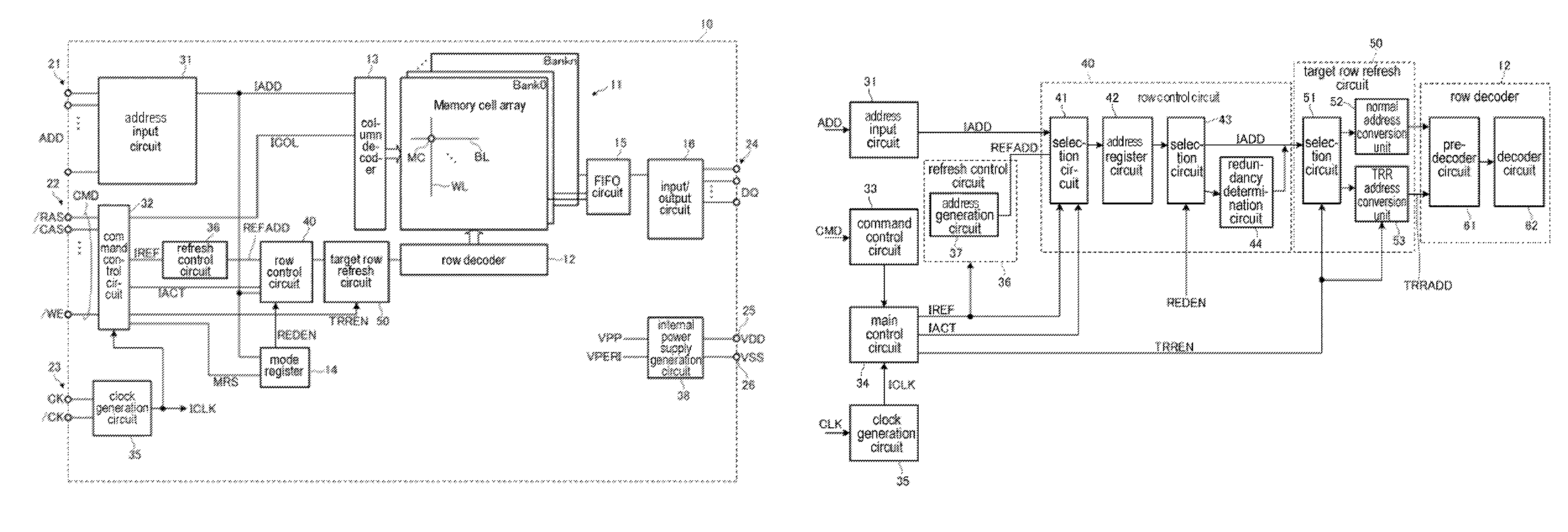
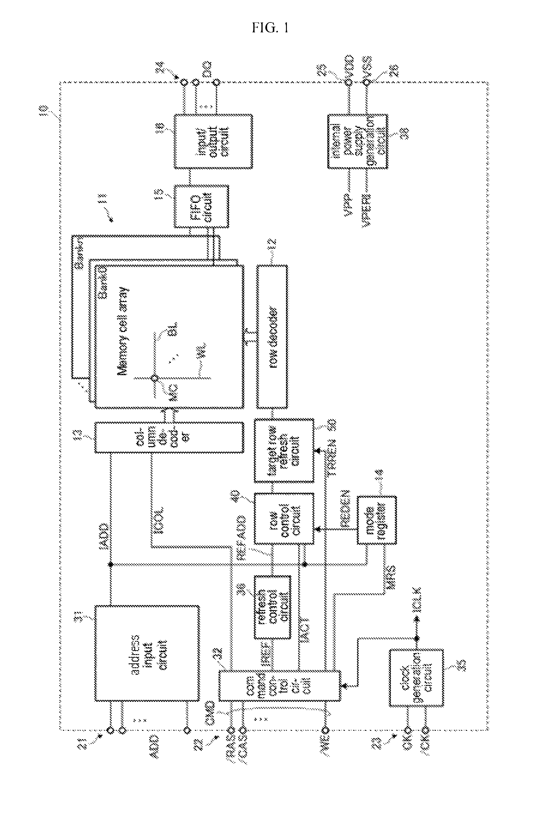
[0063]FIG. 3 is an enlarged circuit diagram of a portion of the memory cell array 11 of the present invention.
[0064]As illustrated in FIG. 3, The memory cell array 11 includes a plurality of word lines WL that run in the Y direction, a plurality of bit lines BL that run in the X direction, and a plurality of memory cells MC arranged at the intersections between the word lines WL and the bit lines BL. The memory cells MC are so-called DRAM cells, and each includes a cell transistor Tr made using an n-channel MOS transistor that is connected in series to a cell capacitor C. The gate electrode of the cell transistor Tr is connected to the corresponding word line WL, and either the source electrode or the drain electrode is connected to the corresponding bit line BL. The other source / drain electrode is connected to the cell capacitor C.
[0065]Each memory cell MC stores data using an electrical charge stored on the cell capacitor C. More specifically, the cell capacitor C is charged usin...
embodiment 2
[0098]Next, Embodiment 2 of the present invention will be described.
[0099]FIG. 11 is a plan view schematically illustrating a configuration of a memory cell array 11 according to Embodiment 2 of the present invention.
[0100]As illustrated in FIG. 11, in the present embodiment word lines WL corresponding to pairs of cell transistors Tr that each share a bit line contact BLC (such as the word lines WLn(0) and WLn(1)) are arranged close to one another with a width W1 therebetween. The bit line contacts BLC are conductive contacts for connecting either the source or drain electrode of each cell transistor Tr to a respective bit line BL. The other source / drain electrode of each cell transistor Tr is connected via a cell contact CC to a cell capacitor C (not illustrated in the figure).
[0101]Meanwhile, adjacent word lines WL corresponding to cell transistors Tr that do not share bit line contacts BLC (such as the word lines WLn(1) and WLn+1(0)) are arranged with a width W2 therebetween, whe...
embodiment 3
[0113]Next, Embodiment 3 of the present invention will be described.
[0114]FIG. 14 is a block diagram of a TRR address conversion unit 53 used in Embodiment 3. Word lines that are positioned on boundaries 150 as illustrated in FIG. 15 require a special conversion process to obtain the logical addresses of the corresponding redundant word lines. This is because different logical address assignment conventions are used in the normal areas (from WL0 to WL7 and from WL8 to WL15 in FIG. 15) and the redundant area (from REDWL0 to REDWL3 in FIG. 15).
[0115]As illustrated in FIG. 15, here the word lines that are positioned on the boundaries 150 are WL7, REDWL0, REDWL3, and WL8. The word lines that are not positioned on the boundaries 150 in FIG. 15 are WL0 to WL6, REDWL1, REDWL2, and WL9 to WL15.
[0116]The TRR address conversion unit 53 includes a boundary address determination circuit 531, a normal TRR address conversion unit 532, and a special TRR address conversion unit 533. The boundary ad...
PUM
 Abstract
Description
Claims
Application Information


