Reference line and bit line structure for 3D memory

a reference line and bit line technology, applied in the field of memory devices, can solve the problems of low yield, inability to read and program data, and inability to meet the requirements of data storage density,

Active Publication Date: 2016-08-09
MACRONIX INT CO LTD
View PDF33 Cites 121 Cited by
  • Summary
  • Abstract
  • Description
  • Claims
  • Application Information

AI Technical Summary

Benefits of technology

[0009]A 3D array of U-shaped NAND strings comprising series-connected even and odd memory cells is described. Even memory cells are disposed in the interface regions accessible via the active pillars and conductive strips in the even stacks of conductive strips. Odd memory cells are disposed in the interface regions accessible via the active pillars and conductive strips in the odd stacks of conductive strips. A top frustum of the active pillar includes a first switch on the even side controlled by a signal on a top strip in the even stack, and a second switch on the odd side controlled by a signal on a top strip in the odd stack. The first switch (e.g. the gate select transistor) can be used to connect the NAND string to a reference line, acting as

Problems solved by technology

These multiple-bit-per-cell programming technologies require fine control over threshold voltages, making read and program disturb characteristics even more critical.
Therefore, even with high-density three-dimensio

Method used


Image

  • Reference line and bit line structure for 3D memory
  • Reference line and bit line structure for 3D memory
  • Reference line and bit line structure for 3D memory

Examples


Embodiment Construction

[0032]A detailed description of embodiments of the present application is provided with reference to the FIGS. 1-27.

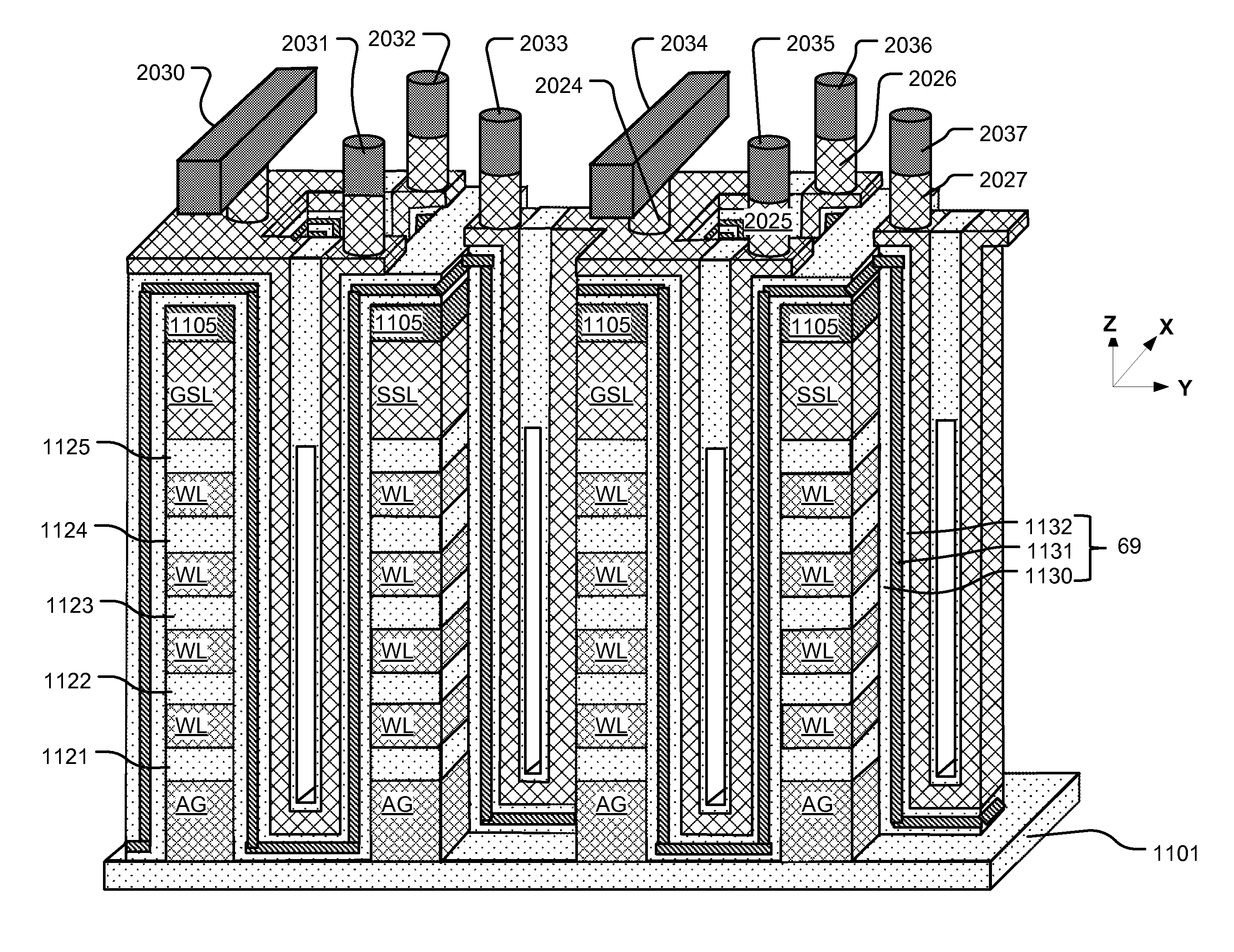
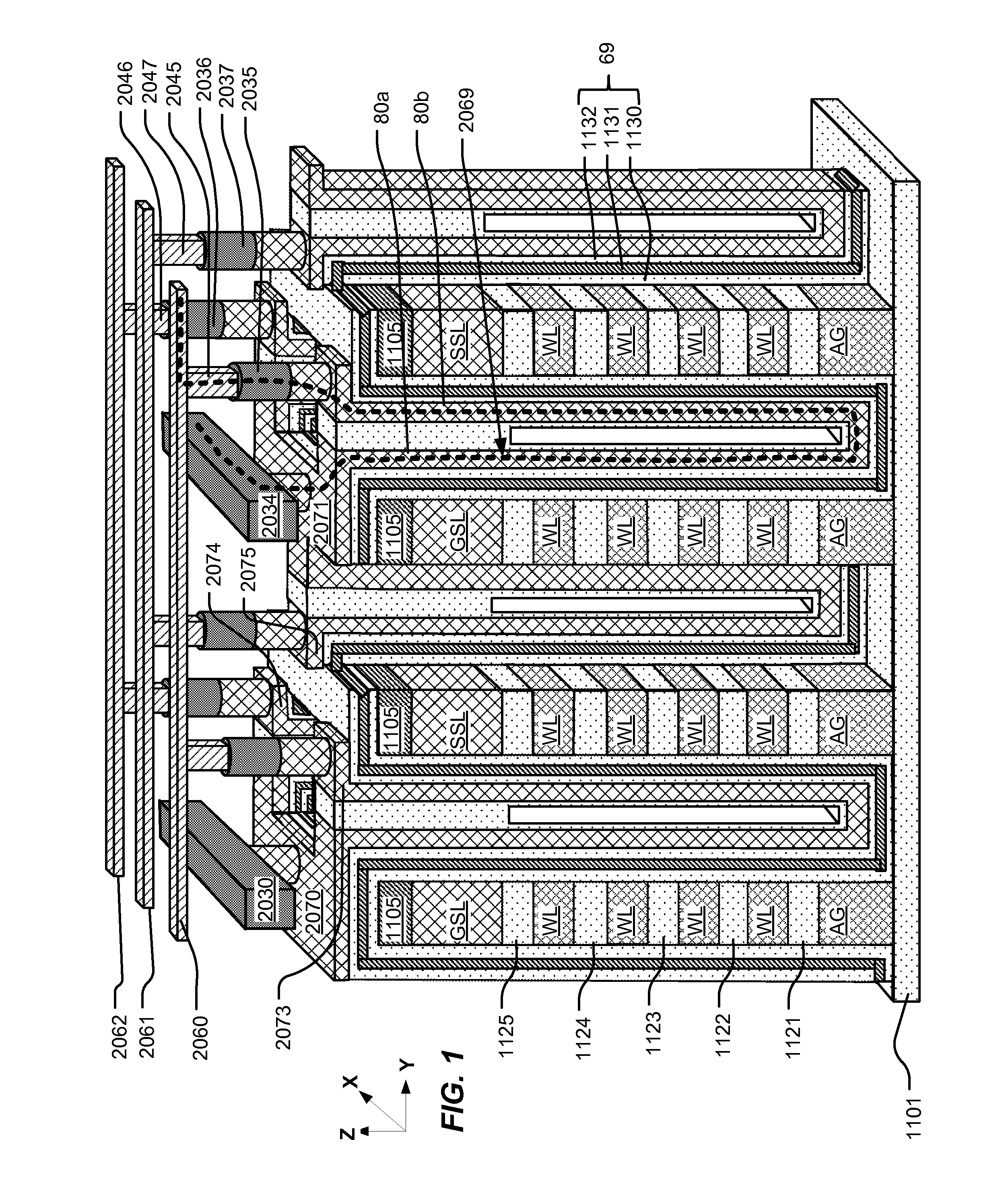
[0033]FIG. 1 is a perspective view of a three-dimensional 3D memory device. The memory device described herein comprises a plurality of stacks having alternating layers of conductive strips (GSL, SSL, WL, AG) and insulating material (1121-1125), data storage structures 69 disposed on the sides of the stacks, and vertical channel films 80a / 80b contacting data storage structures 69. Over the stacks are disposed common source lines, such as reference lines 2030, 2034, and bit lines 2060-2062. Circuit path 2069 shows the current flow for a U-shaped NAND string. The combination of vertical channel films 80a / 80b and data storage structures 69 is referred to herein as an active pillar.

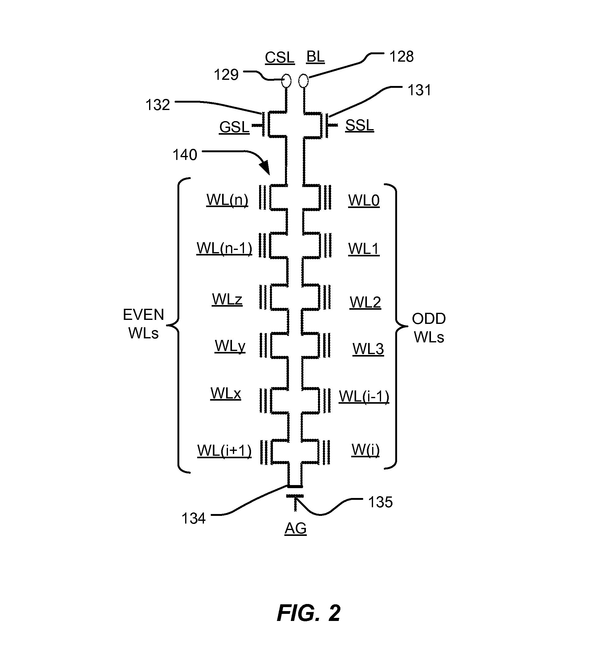
[0034]FIG. 2 shows a circuit schematic for a U-shaped NAND, corresponding to the circuit path 2069 from reference line 2034 to bit line 2060 shown in FIG. 1. The U-shaped NAND string is connecte...


PUM


Abstract

A 3D NAND flash memory includes even and odd stacks of conductive strips. Some of the conductive strips in the stacks are configured as word lines. Data storage structures are disposed on the sidewalls of the even and odd stacks. Active pillars include even and odd semiconductor films on the data storage structures connected at the bottom ends so that the semiconductor films can be thin films having a U-shaped current path. An even pad connected to the even semiconductor film and an odd pad connected to the odd semiconductor film are disposed over the even and odd stacks respectively. A segment of a reference line is connected to the even pad, and an inter-level connector is connected to the odd pad. A segment of a bit line comprises an extension contacting the inter-level connector.

Description

BACKGROUND[0001]1. Technical Field[0002]The present application relates to memory devices, and particularly to 3D array memory devices in which bit lines and common source lines are arranged to provide a simple routing structure.[0003]2. Description of Related Art[0004]As critical dimensions of devices in integrated circuits shrink to the limits of common memory cell technologies, designers look for techniques to stack multiple levels of memory cells to achieve greater storage capacity and lower costs per bit. For example, thin film transistor techniques are applied to charge trapping memory technologies in Lai et al., “A Multi-Layer Stackable Thin-Film Transistor (TFT) NAND-Type Flash Memory,” IEEE Int'l Electron Devices Meeting, 11-13 Dec. 2006; and in Jung et al., “Three Dimensionally Stacked NAND Flash Memory Technology Using Stacking Single Crystal Si Layers on ILD and TANOS Structure for Beyond 30 nm Node,” IEEE Int'l Electron Devices Meeting, 11-13 Dec. 2006.[0005]Another str...

Claims


Application Information

Patent Timeline
IPC IPC(8): H01L27/115H01L27/105
CPCH01L27/11565H01L27/1157H01L27/11582H01L27/1052H10B41/20H10B41/27H01L29/42348H01L29/40117H10B43/27H10B43/10
Inventor YEH, TENG-HAOHU, CHIH-WEIJIANG, YU-WEI
Owner MACRONIX INT CO LTD
Why Eureka
Try Eureka