
Junctionless tunnel fet with metal-insulator transition material

a transition material and junctionless tunnel technology, applied in the direction of basic electric elements, electrical apparatus, semiconductor devices, etc., can solve the problems of limited sub-threshold slope (i.e., change of gate voltage required), and achieve uniform doping profile, increase the electric field and conductivity

Inactive Publication Date: 2016-08-16
IBM CORP
View PDF29 Cites 5 Cited by
  • Summary
  • Abstract
  • Description
  • Claims
  • Application Information

AI Technical Summary

Benefits of technology

The present disclosure provides an integrated circuit (IC) structure that includes a doped semiconductor layer with a uniform doping profile, a first gate structure positioned on the doped semiconductor layer, and a second gate structure positioned on the doped semiconductor layer. The second gate structure includes a metal-insulator transition material and a gate dielectric layer separating the metal-insulator transition material from the doped semiconductor layer. The second aspect provides a method of forming an integrated circuit (IC) structure. The third aspect provides an integrated circuit (IC) structure that includes a doped semiconductor layer with a uniform doping profile, a first gate structure contacting the doped semiconductor layer, and a second gate structure contacting the doped semiconductor layer. The second gate structure includes a second gate material including a metal-insulator transition material therein, and the dielectric layer, wherein a voltage bias applied to the first gate structure increases the electric field and a conductivity of the metal-insulator transition material. The technical effects are designed to provide improvements in the performance and functionality of integrated circuits.

Problems solved by technology

Although a junctionless FET is relatively simple to fabricate, the sub-threshold slope (i.e., the change in gate voltage required to increase the source to drain current by one order) may be limited due to conventional over the barrier carrier transport.
A tunnel FET may have limited opportunities for use because fabricating the various semiconductor materials and introducing dopants to the buried semiconductor layer can increase manufacturing costs and complexity.

Method used


Image

  • Junctionless tunnel fet with metal-insulator transition material
  • Junctionless tunnel fet with metal-insulator transition material
  • Junctionless tunnel fet with metal-insulator transition material

Examples


Embodiment Construction

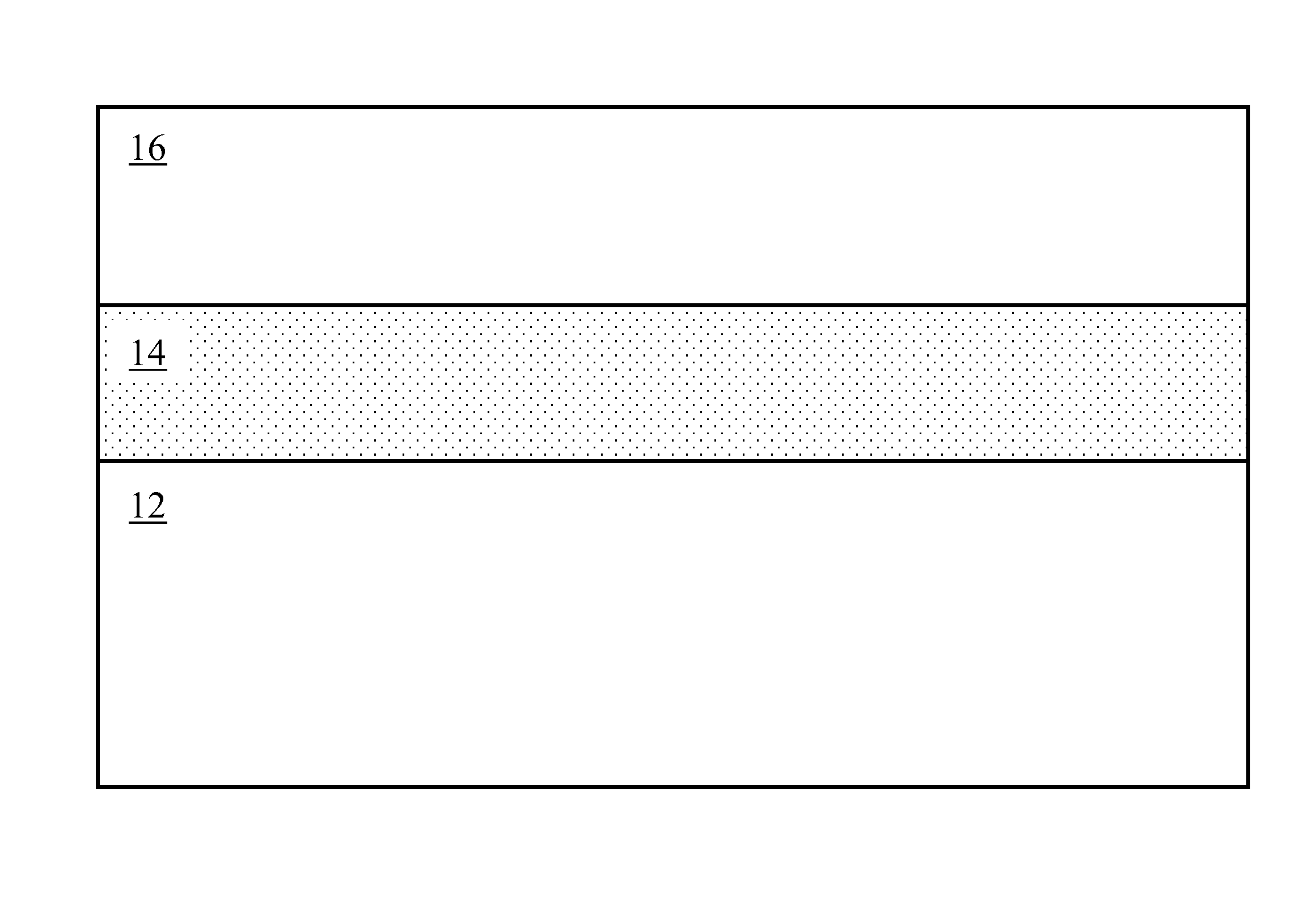
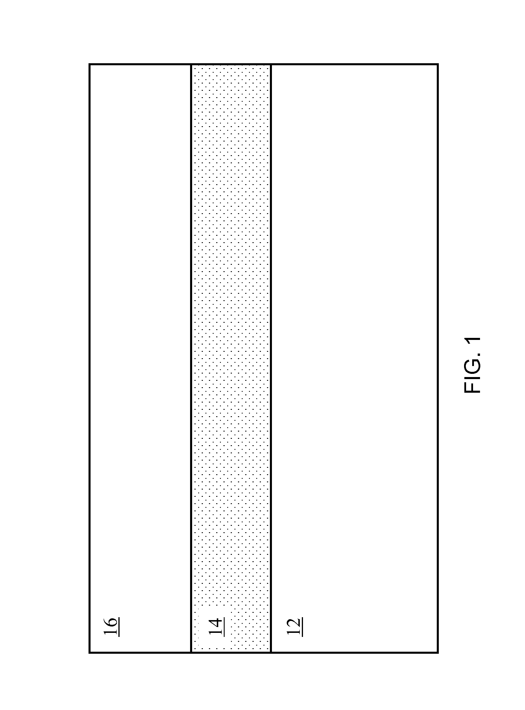
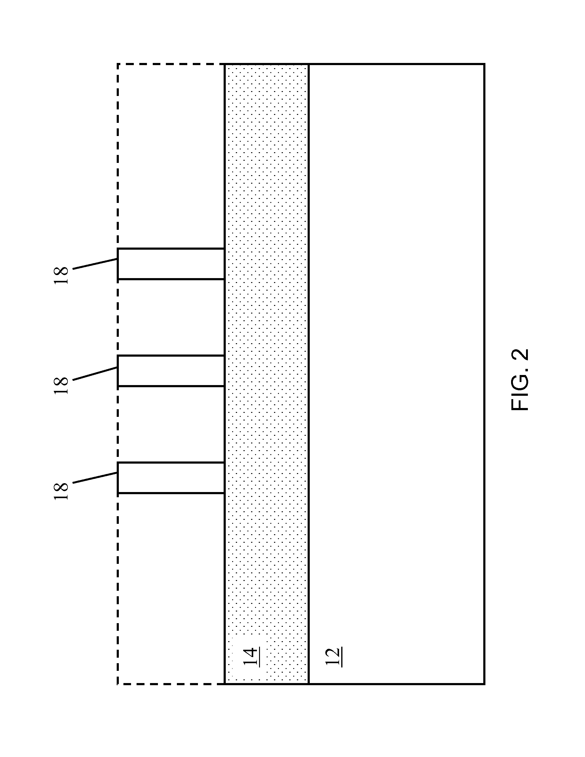
[0012]Embodiments of the present disclosure provide an integrated circuit (IC) structure which, in operation, can have a lower sub-threshold slope (i.e., the change in gate voltage required to increase the source to drain current by one order) than a junctionless FET. In an embodiment, an IC structure of the present disclosure can have a subthreshold slope of less than sixty millivolts (mV) per decade (mV / dec). In addition, embodiments of the present disclosure include a doped semiconductor layer which includes a substantially uniform doping profile.

[0013]Embodiments of the present disclosure can include a doped semiconductor layer with a “substantially uniform” doping profile therein. As used herein, the term “substantially uniform” refers to a concentration of dopants (measured, e.g., in atoms per cubic centimeter) which is either uniform throughout a material or includes insignificant variances in concentration, such that the doped semiconductor layer is indistinguishable from a ...


PUM


Abstract

Embodiments of the present disclosure provide an integrated circuit (IC) structure, which can include: a doped semiconductor layer having a substantially uniform doping profile; a first gate structure positioned on the doped semiconductor layer; and a second gate structure positioned on the doped semiconductor layer, the second gate structure including a metal-insulator transition material and a gate dielectric layer separating the metal-insulator transition material from the doped semiconductor layer.

Description

BACKGROUND[0001]The disclosure relates generally to structures and manufacturing processes for junctionless tunnel field effect transistors (FETs). More specifically, embodiments of the present disclosure include a junctionless tunnel FET structure with a metal-insulator transition material therein, and processes for fabricating the junctionless tunnel FET structure.[0002]In integrated circuit (IC) structures, a transistor is a critical component for implementing digital circuitry designs. A conventional transistor includes three electrical terminals: a source, a drain, and a gate. By applying different voltages to the gate terminal, the ability for electric current to flow between the source and the drain can be turned on and off. A common type of transistor is a field effect transistor (FET). A FET can include a gate structure, typically composed of polysilicon and / or a metal, formed on and contacting an insulator placed on top of the semiconductor layer positioned between the sou...

Claims


Application Information

Patent Timeline
Patent Type & Authority Patents(United States)
IPC IPC(8): H01L29/02H01L29/10H01L29/78H01L29/66H01L29/51
CPCH01L27/1211H01L29/66977H01L29/517H01L29/42364H01L21/845H01L29/7855H01L29/1033H01L29/511H01L29/42372H01L29/4908H01L29/0673H01L49/003H01L29/66795H01L29/78645H01L29/78648H01L29/775H01L29/7831H01L2029/7857H10N99/03
Inventor BAJAJ, MOHITGUNDAPANENI, SURESHKONAR, ANIRUDDHAMURALI, KOTA V. R. M.NOWAK, EDWARD J.
Owner IBM CORP
Learn More